LVGL
LVGL is an open-source embedded graphics library used for creating beautiful, high-performance, and customizable graphical user interfaces (GUIs). It is designed to be simple and flexible, making it suitable for various embedded platforms, including microcontrollers and microprocessors.
Requirements
The sample supports the following development kits:
Hardware Platforms |
Board Name |
Build Target |
|---|---|---|
RTL87x3E EVB |
|
|
RTL87x3E HDK |
RTL87x3E EVB |
|
RTL87x3D HDK |
RTL87x3D EVB |
|
Note
To purchase EVB, please visit https://www.realmcu.com/en/Home/Shop.
When built for an xxx_16M_xxx build target, the sample is configured to build and run with a 16M flash map.
To quickly set up the development environment, please refer to the detailed instructions provided in Quick Start.
Touchpad and LCD
The default supported touch screen and LCD models in the application are listed in the following table:
Board Name |
Touchpad |
LCD |
|---|---|---|
RTL87x3E EVB |
CHSC6417 |
SH8601Z |
RTL87x3D EVB |
CHSC6417 |
ST7801 |
RTL87x3EP EVB |
CHSC6417 |
SH8601Z |
For convenience in testing the touchpad and LCD, we have developed an adapter board. Simply plug the adapter board into the card slot of the EVB, and it is possible to test and use the touchpad and LCD.
RTL87x3E and RTL87x3EP EVB
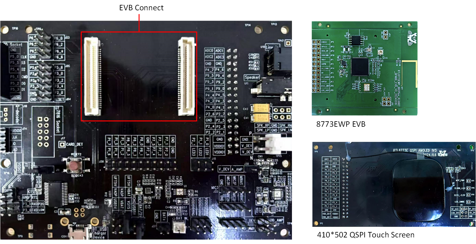
RTL87x3EP EVB Touch Screen and LCD Model for RTL87x3E or RTL87x3EP
The mapping relationship between the touchpad or LCD and EVB pins is shown in the following table:
Touchpad and LCD |
EVB |
|---|---|
TP_SCL |
ADC_0 |
TP_SDA |
ADC_1 |
TP_INT |
ADC_2 |
TP_RST |
ADC_3 |
SPI_CLK |
P9_4 |
SPI_SIO3 |
P9_5 |
SPI_CSN |
P9_2 |
SPI_SIO0 |
P9_3 |
SPI_SIO2 |
P9_0 |
SPI_SIO1 |
P9_1 |
LCD_RST |
P4_4 |
TE |
P2_2 |
VCI_EN |
P4_3 |
RTL87x3D EVB
The touch screen and LCD model are connected to the EVB via an adapter board. Simply plug the adapter board into ‘CON4’ of the EVB.
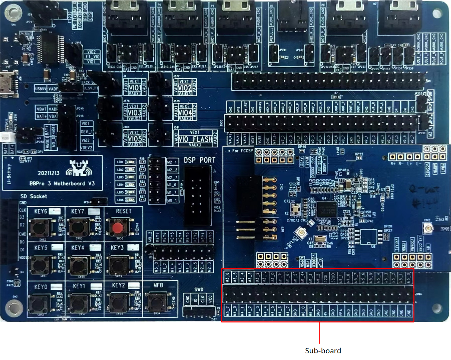
RTL87x3D EVB
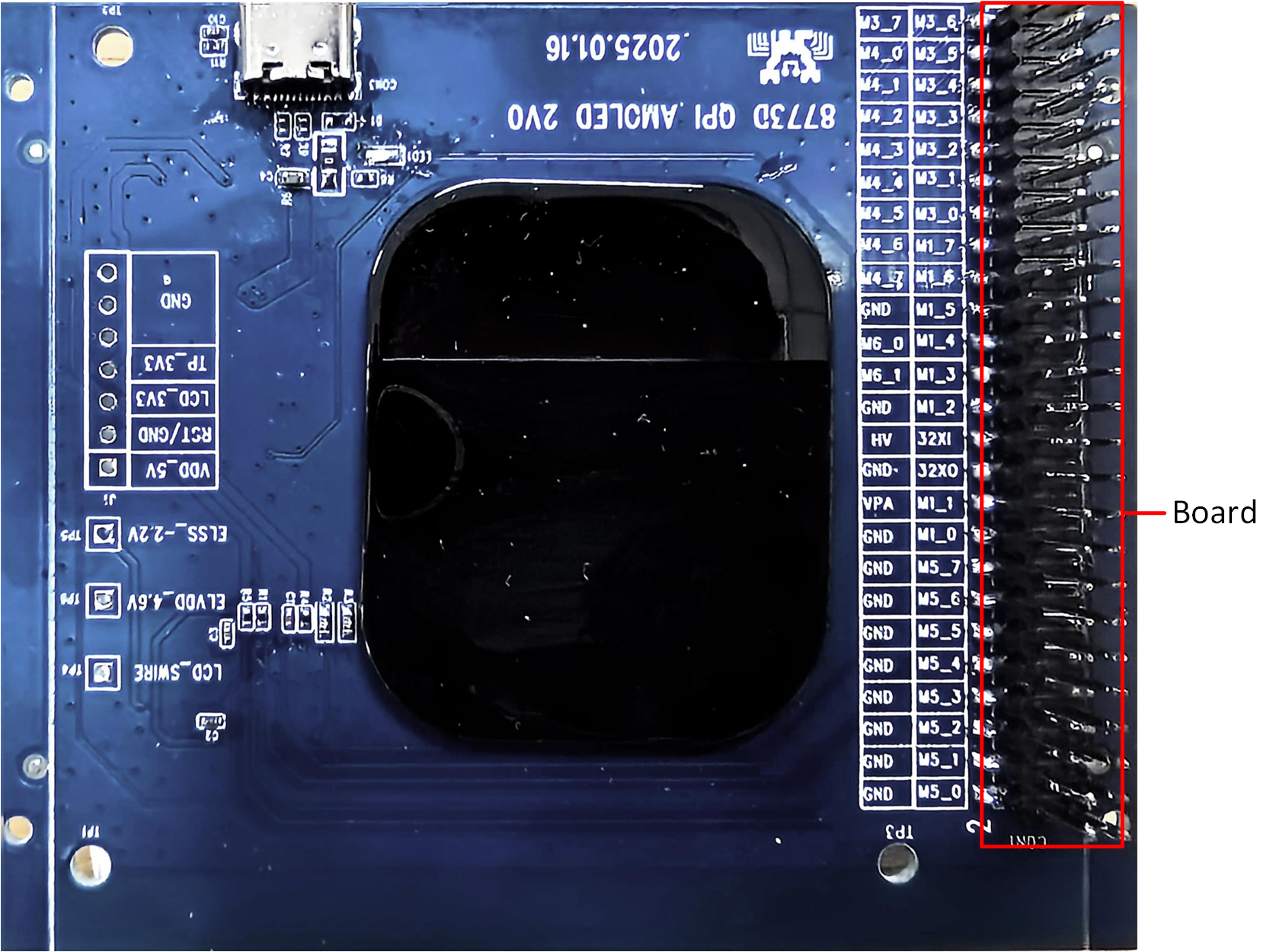
Touch Screen and LCD Model for RTL87x3D
The mapping relationship between the touchpad or LCD and EVB pins is shown in the following table:
Touchpad and LCD |
EVB |
|---|---|
TP_SCL |
M4_5 |
TP_SDA |
M4_6 |
TP_INT |
M4_4 |
TP_RST |
M4_2 |
SPI_CLK |
M3_2 |
SPI_SIO3 |
M3_7 |
SPI_CSN |
M3_3 |
SPI_SIO0 |
M3_4 |
SPI_SIO2 |
M3_6 |
SPI_SIO1 |
M3_5 |
LCD_RST |
M5_2 |
TE |
M5_4 |
VCI_EN |
M5_5 |
Tools
SDK provides image conversion tools that facilitate the conversion of images, such as JPG, PNG , BMP , into burnable binary files. The image conversion tool provided by the SDK is located in the sdk\tool\ path. The interface of the image conversion tool is as follows:
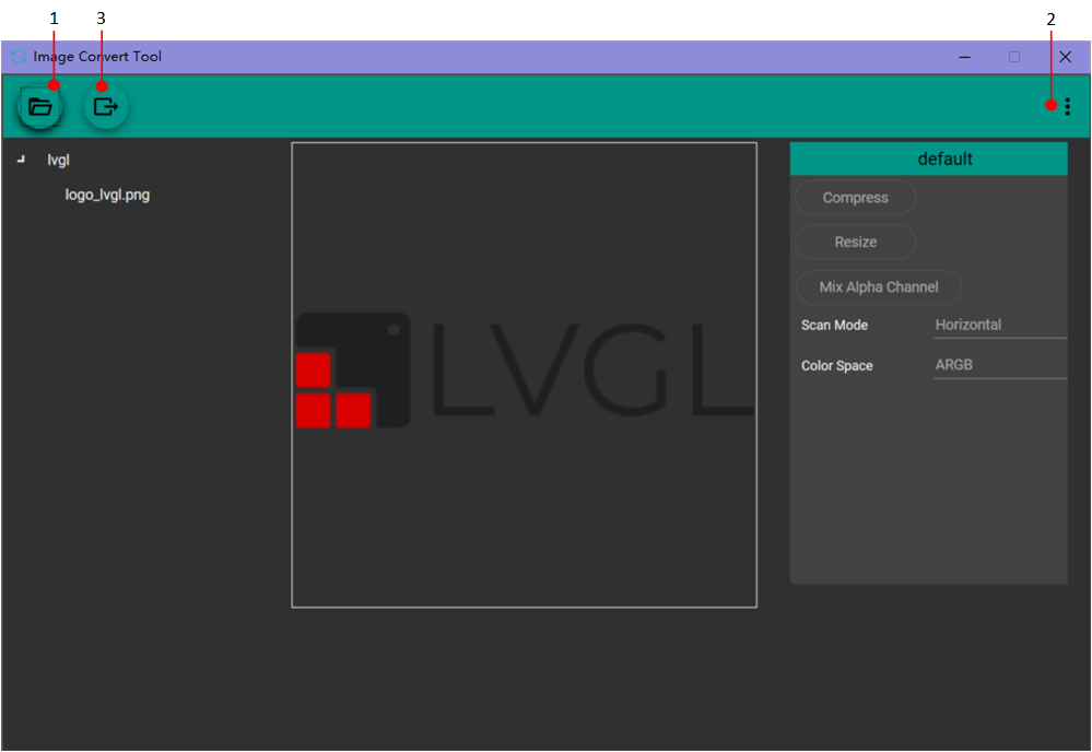
Image Convert Tool
Import the directory to be converted.
Set the conversion format: Choose whether to compress, output image color space format, output image properties (JPG, PNG, BMP), output image save location, and other parameters.
Convert the images.
If users want to learn more about the tool’s usage guidelines, more information can be found in the introduction documentation for the Image Convert Tool in the sdk\doc\EN directory.
Files
The previous chapter introduced the steps for converting image resources. For font resource conversion, it is necessary to consult with FAE to address the requirements. Once both the image and font resources have been generated as binary files, the package tool can be used to convert them into the final userdata binary file.
The GUI package tool provided by the SDK is located in the sdk\tool\Gadgets\gui_package_tool path. Select the folder according to the IC type.
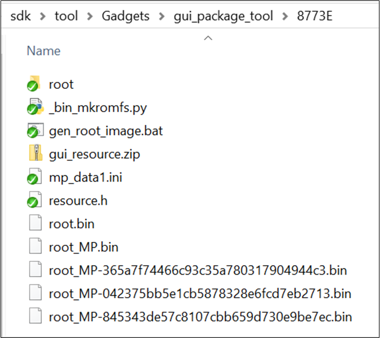
GUI Package Tool
Place the binary files of the images and fonts into the root folder.
Execute the
gen_root_image.bat.A userdata binary file will be generated in the current path. Please select the file with the suffix and random number.
While packing the userdata file, a resource.h file will also be generated. This file is used to generate the APP binary file, and the APP code can use the addresses of the images or fonts in this file to index the related resources.
Configurations
The configuration of the LVGL solution in the SDK is located in SDK\board\evb\lvgl\menu_config.h, you can check them in Configuration Wizard of Keil, the default configuration is as follows:
// <e> HoneyGUI Enable LVGL
#define CONFIG_REALTEK_BUILD_LVGL_V8      1
#define CONFIG_REALTEK_BUILD_LVGL_V9      0

#if (CONFIG_REALTEK_BUILD_LVGL_V8 == 1) || (CONFIG_REALTEK_BUILD_LVGL_V9 == 1)

// <c> HoneyGUI Enalbe LVGL APP
#define CONFIG_REALTEK_BUILD_LVGL_DEMO_APP
// </c>

// <c> HoneyGUI Enable LVGL EXAMPLES
#define CONFIG_REALTEK_BUILD_LVGL_EXAMPLES
// </c>

// <c> HoneyGUI Enable LVGL RLOTTIE
// #define CONFIG_REALTEK_BUILD_LVGL_RLOTTIE
// </c>

#endif
Building and Downloading
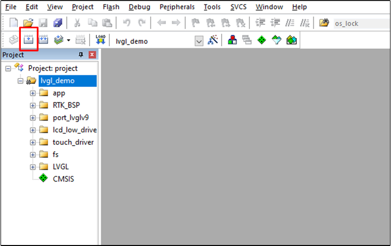
This application can be found under SDK\board\evb\lvgl\mdk in SDK folder structure.
This sample can be found under board\evb\lvgl_demo in the SDK folder structure.
Take the project project.uvprojx and target lvgl_demo as an example, to build and run the sample with Keil development environment, follow the steps listed below:
Reference Quick Start to build and download. It is worth noting that:
Open
rtl87x3e_gui_demo.uvprojx.-
Building Keil MDK project , Generating APP Image section:
The LVGL SDK project path is
SDK\board\evb\lvgl.The Keil MDK project path is
SDK\board\evb\lvgl\mdk.After modifying the project configuration, you need to rebuild the project configuration for the changes to take effect. After the build, a completely new project file will be generated based on the configuration, replacing the original project file. If the developer manually added files or configurations to the original project, those modifications will become invalid and won’t be retained in the new project.
-
To build the project, open a cmd window in the project path.
Run the command scons --target=mdk5 to build the mdk project. Open the mdk project for compilation.
SDK\board\evb\lvgl> scons --target=mdk5
scons: Reading SConscript files ...
...
CC xxxx.o
CC xxxx.o
...
LINK rtl8773e_lvgl_demo.elf
fromelf --binary rtl8773e_lvgl_demo.elf --output rtthread.binary
fromelf -z rtl8773e_lvgl_demo.elf
scons: done building targets.
-
Open the generated Keil MDK project and click on Build(F7) to generate the APP image. Refer to Generating APP Image section.
Building
After a successful compilation, the APP binary file
lvgl_demo_bank0_MP-v0.0.0.0-xxx.binarywill be generated in the directorybinary\rtl87x3e\flash_16M\bank0.
For downloading and programming methods, please refer to Images Download.
Generating and downloading User Data.
Note
Be sure to place the SDK, tools, and other materials in non-Chinese paths, and ensure that all images in the aforementioned paths are loaded into the tool and burned together.
The SDK also provides a default binary for the LVGL APP binary
lvgl_demo_bank0_MP-va.b.c.d-yyyyyyyyin the directorybinary\rtl87x3ep\app_demo_bin\mdk\lvgl\16M\BANK0. Users can directly use this default file without modifying any code.
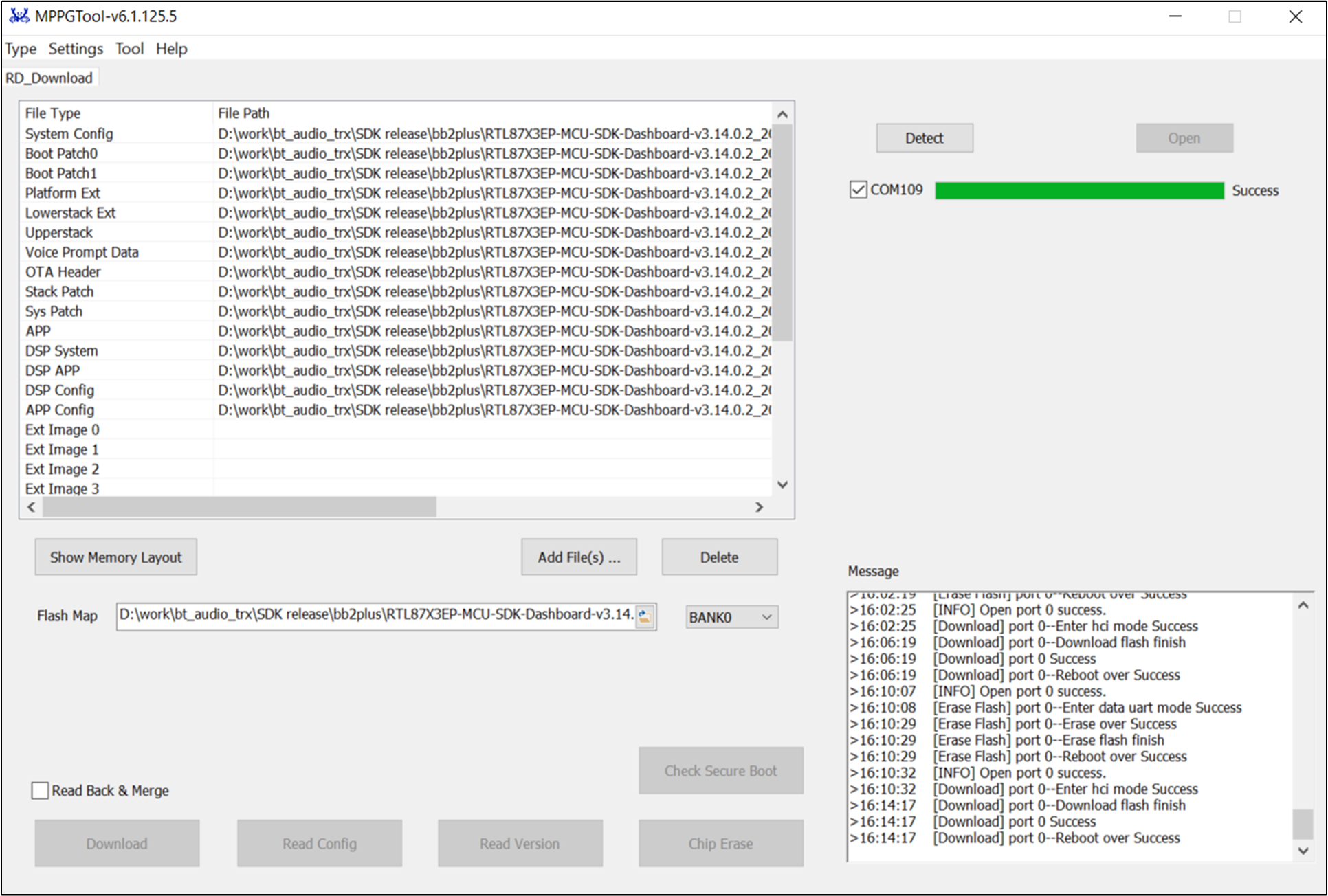
Download All Images
Press the Reset button on the EVB board.
J-Link Download and Debug
J-Link is an emulator/debugger developed by SEGGER. It is a tool specifically for ARM processors that can be used to develop, debug, and test firmware for embedded devices. J-Link has high-speed and reliable simulation performance, supports real-time debugging and fast firmware downloading, and can help developers speed up the process of debugging and verifying embedded systems and improve development efficiency and quality.
J-Link supports multiple connection interfaces, such as JTAG, SWD, etc. Because SWD uses fewer wires, RTL8773EWP uses this interface, SWD corresponding interface. In addition, J-Link is also compatible with multiple development environments and IDEs (such as Keil MDK, IAR Embedded Workbench, etc.). For Keil environment settings, please refer to Quick Start to build and download.
It is recommended to use J-Link Software v6.44 (or later). For more information, please reference Quick Start to build and download.
SWD Wiring
RTL8773EWP |
SWD |
|---|---|
GND |
GND |
P1_0 |
SWIO |
P1_1 |
SWCK |
VDEX |
Vterf/3.3V |
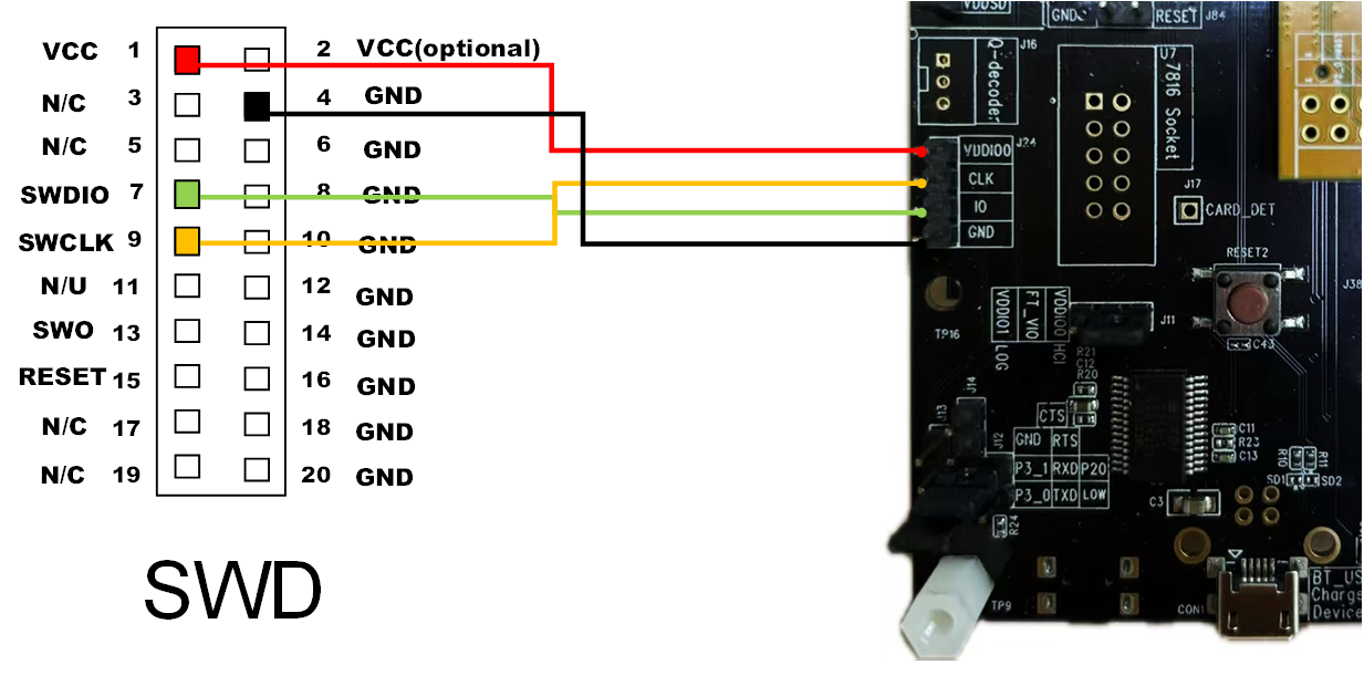
J-Link Pinmux on EVB
Experimental Verification
LVGL Testing
After successfully flashing the firmware and UserData, switch the EVB to working mode and perform a reset to restart.
After the device restarts, you will see LVGL benchmark demo is running, it witll display the current test case and progress in the top left corner of the screen, and show the current frame rate and CPU usage in the bottom right corner of the screen.
There will be no log output and no touch screen interaction response until all test cases are completed. After completing all test cases, the test results will be displayed in logs and tables. You can scroll through the touch screen to browse the results.

LVGL UI Demo on PC Simulator
Code Overview
This chapter provides an overview of the software-related technical specifications and behavior specifications for the RTL8773EWP LVGL solution.
Source Code Directory
Project directory:
sdk\board\evb\lvgl\mdk.Source code directory:
sdk\board\evb\lvgl\src.
Source files in LVGL application project are currently categorized into several groups as below:
└── Project: lvgl
    └── app                            includes the LVGL user application implementation
        ├── menu_config.h              project construct configurations
        ├── app_lower_init.c           includes task and hardware init
        ├── lvgl_demo.c                includes LVGL demo, benchmark demo
        ├── main.c
        └── simkai_size32_bits1_font.c
    ├── RTK_BSP
    ├── module
    ├── fs                              include file system implementation
    ├──  port_lvglv9
        ├── lv.conf.h                   includes LVGL configurations
        ├── lv_port_disp.c              includes LVGL display interface
        ├── lv_port_indev.c             includes LVGL input device interface
        └── lv_port_fs.c                includes LVGL filesystem interface
    └── lvgl_assets                     includes user image and font C files
        ├── img_demo_lvgl_logo.c        lvgl logo image array
        ├── logo_lvgl_rle.c             lvgl logo image rle array
        ├── lv_font_harmony_32.c        harmony font array
        └── lvgl_example_assets.c       example shows how to set image and font source
    └── LVGL                            includes all LVGL source
    └── CMSIS
Flash Layout
Application default flash layout header file: sdk\binary\rtl87x3ep\flash_map_config\16M\flash_16M\flash_map.h.
Example Layout with a Total Flash Size of 16MB |
Size(Byte) |
Start Address |
|---|---|---|
EQ_Fitting |
4K |
0x02000000 |
Reserve |
7K |
0x02000400 |
OEM Config |
5K |
0x02002000 |
Bank0 Boot Patch |
12K |
0x02004000 |
Bank1 Boot Patch |
12K |
0x02007000 |
Platform |
20K |
|
Lowerstack |
28K |
|
Upperstack |
252K |
|
OTA Bank0 |
1760K |
0x02055000 |
|
1K |
0x02055000 |
|
163K |
0x02055400 |
|
104K |
0x0207E000 |
1136K |
0x02098000 |
|
|
128K |
0x021B4000 |
|
200K |
0x021D4000 |
|
20K |
0x02206000 |
|
8K |
0x0220B000 |
|
0K |
0x00000000 |
|
0K |
0x00000000 |
|
0K |
0x00000000 |
|
0K |
0x00000000 |
OTA Bank1 |
1760K |
0x0220D000 |
VP Data |
200K |
0x023C5000 |
FTL |
84k |
0x02FE9000 |
BKB DATA1 |
0 |
0x00000000 |
BKB DATA2 |
8k |
0x02FFE000 |
APP Defined Section |
60K |
0x02400000 |
User Data1 |
9860K |
0x0240f000 |
Important
To adjust flash layout, flow the steps listed on the Generating Flash Map in reference Quick Start.
After flash layout adjustment, users must flow the steps listed on the Generating OTA Header and Generating MCU Configuration File with new
flash_map.ini.
Software Architecture
The system software architecture is shown below:
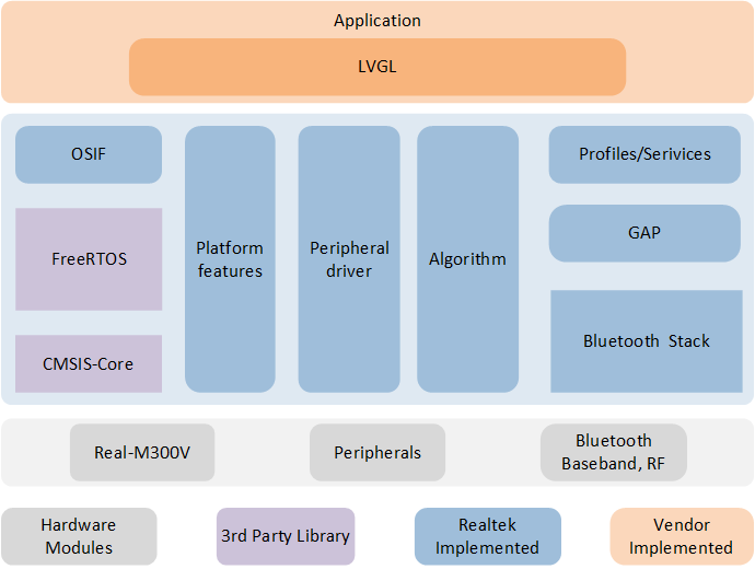
Software Architecture
Tasks and Priorities
RTL8773EWP uses RTOS by default, and encapsulates a layer of OS if interface on this basis. RTL8773EWP has built-in Timer task, Idle task, Flash task, Bluetooth controller Stack task, Bluetooth Host Stack task, and the LVGL application has its own APP task, GUI task, Communication Send task, and Communication Receive task.
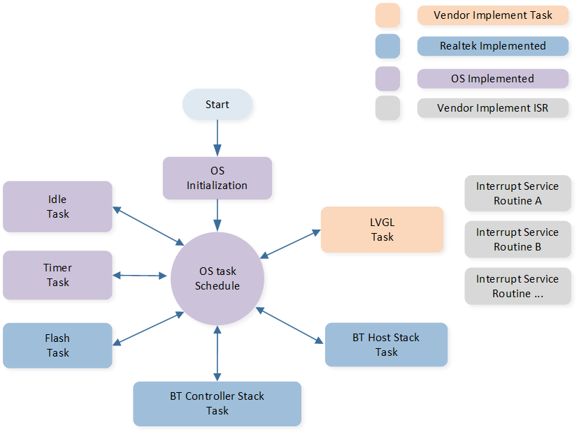
LVGL Application Task Composition
Task |
Description |
Priority |
|---|---|---|
Timer |
Implement software timers as required by FreeRTOS. |
6 |
Bluetooth Controller Stack |
Implement the Bluetooth protocol stack below the HCI layer. |
6 |
Bluetooth Host Stack |
Implement the Bluetooth protocol stack above the HCI layer. |
3 |
Flash |
Handle asynchronous flash requests. |
1 |
Idle |
Run background tasks, including DLPS. |
0 |
LVGL Task |
Process image generation and screen data transmission. |
1 |
Note
Multiple application tasks can be created, and memory resources will be allocated accordingly.
Idle tasks and timer tasks are provided by FreeRTOS.
Tasks have been configured to be preemptive based on their priority using the SysTick interrupt.
Interrupt Service Routines (ISR) have been implemented by the vendor.
APP task initialization related code entry:
int main(void)
{
    APP_PRINT_INFO0("LVGL demo");
    APP_PRINT_INFO2("APP COMPILE TIME: [%s - %s]", TRACE_STRING(__DATE__), TRACE_STRING(__TIME__));
    system_lower_init();

#if (TARGET_RTL8773DO == 1)
    app_io_resource_request_init();
#endif
#if (LCD_INTERFACE == LCD_INTERFACE_QSPI)
    lcd_pin_config(LCD_RST);
#endif
#if (TARGET_LCD_DEVICE == LCD_DEVICE_ST7801)
    lcd_vci_en_pin_config(VCI_EN);
#endif
#if (ENABLE_TE_FOR_LCD == 1)
    lcd_te_pin_config(LCD_TE);
#endif

    rtk_lcd_hal_init();

    extern int rt_lvgl_demo_init(void);
    rt_lvgl_demo_init();

    os_sched_start();

    return 0;
}
LVGL Task
UI
The main configuration items for LVGL are configured in sdk\board\evb\lvgl\src\lvgl_port\lv_conf.h, including display device size, color depth, stack interface configuration, and more. Developers can customize these settings according to their needs.
For guidelines on designing and developing the LVGL UI, please refer to Use LVGL Design An Application and the LVGL online documentation LVGL Documentation. The document Use LVGL Design An Application provides detailed instructions on using a PC simulator, methods for real device porting, benchmark performance, UI resource conversion, and basic LVGL development methods. The document LVGL Documentation contains LVGL development documentation, detailing its features and functionalities, along with numerous examples.
Troubleshooting
PPPE2.0 Performance Measurement
As shown below, seven tasks have been created for the user application:
-
Single input layer 480*480 ARGB8888 matrix 2x2, unit matrix; output layer 480*480 ARGB8888.
PPPE2.0 Performance Measurement Color Format ARGB8888 Path Number
Data Path
Measured Time (ms)
Path 1
SRAM -> PPE -> SRAM
9.20
Path 2
SRAM -> PPE -> SRAM
27.65
Path 3
SRAM -> PPE -> SRAM
9.20
Path 4
PSRAM -> PPE -> SRAM
108.7
Path 5
FLASH -> PPE -> SRAM
184.08
Path 6
SRAM -> PPE -> PSRAM
27.65
Path 7
SRAM -> PPE -> PSRAM
9.20
Path 8
SRAM -> PPE -> SRAM
30.28
Note
Path: XXX->PPE->YYY, where XXX represents the input address of input layer2, and YYY represents the input (old frame)/output (new frame) address of input layer1 and result layer 0.
The SRAM in this table refers to DTCM.
-
Input layer1: color format RGB565, matrix 1x1, unit matrix, area 480*480, share memory with result layer. Input layer2: color format ARGB8565, matrix 2x2, conversion matrix as described above, mirror matrix, area 480*480. Result layer0: color formatRGB565, area 480*480.
PPPE2.0 Performance Measurement Color Format RGB565 Path Number
Data Path
Measured Time (ms)
Path 1
SRAM -> PPE -> SRAM
12.65
Path 2
SRAM -> PPE -> SRAM
51.74
Path 3
SRAM -> PPE -> SRAM
17.92
Path 4
PSRAM -> PPE -> SRAM
112.80
Path 5
FLASH -> PPE -> SRAM
189.83
Path 6
SRAM -> PPE -> PSRAM
54.58
Path 7
SRAM -> PPE -> PSRAM
32.51
Path 8
SRAM -> PPE -> SRAM
64.58
Path 9
PSRAM -> PPE -> PSRAM
164.52
Note
Path: XXX->PPE->YYY, where XXX represents the input address of input layer2, and YYY represents the input (old frame)/output (new frame) address of input layer1 and result layer 0.
The SRAM in this table refers to DTCM.