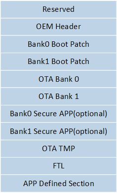
Flash Layout of RTL87x2G consists of Reserved,OEM Header, Bank0 Boot Patch,Bank1 Boot Patch, OTA Bank0, OTA Bank1, OTA TMP,Secure APP(optional),FTL
and APP defined section, the starting address for accessing flash is 0x04000000((The first 4K of flash is Reserved area).
Memory and corresponding function of flash is shown in Flash Memory and Function Description.
Storage of Config information, including Bluetooth address, AES Key and Customizable Flash Layout
No
Bank0 Boot Patch
Variable
(Determined by Efuse)
Variable
(Determined by Efuse)
Flash boot loader.
Bank0 Boot Patch and Bank1 Boot Patch have the same function and serve as backup areas for each other.
Yes
Bank1 Boot Patch
Variable
(Determined by Efuse)
Variable
(Determined by Efuse)
Flash boot loader
Yes
OTA Bank0
Variable
(defined in OEM Config)
Variable
(defined in OEM Config)
OTA Bank0 is primarily used to store the firmware and runtime data of the device. For specific functions, refer to OTA Bank Flash Segmentation.
In the non-support bank switching OTA scheme, the OTA TMP area is used as an OTA backup area to store backup firmware. The BootLoader will eventually copy and activate the backup firmware.
On the other hand, in the supporting bank switching OTA scheme, OTA Bank0 and OTA Bank1 are used as mutually backup firmware storage areas. During the firmware update process,
these two storage areas can be alternately used, ensuring that in the event of a firmware update failure, the system can revert to the previous backup firmware, thereby maintaining system stability and security.
Yes
OTA Bank1
Variable
(defined in OEM Config)
Variable
(defined in OEM Config)
In the supporting bank switching OTA scheme, if OTA Bank0 is the active area, then OTA Bank1 will be the backup area. Conversely, if OTA Bank1 is the active area, then OTA Bank0 will be the backup area.
Yes
Bank0 Secure APP
Variable
(defined in OEM Config)
Variable
(defined in OEM Config)
When TrustZone is enabled, Secure APP (Secure Application) can run in the TrustZone environment, ensuring the security protection of sensitive data and operations.
In this case, Bank0 Secure APP and Bank1 Secure APP have the same function and act as backup areas for each other.
Yes
Bank1 Secure APP
Variable
(defined in OEM Config)
Variable
(defined in OEM Config)
Same as Bank0 Secure APP, serving as a backup area for each other
Yes
OTA TMP
Variable
(defined in OEM Config)
Variable
(defined in OEM Config)
If you are not using bank switching for OTA updates, and instead using one bank as the backup area, then the size of the backup area must be equal to or greater than the maximum size of the image stored in OTA bank0.
Yes
FTL
Variable
(defined in OEM Config)
Variable
(defined in OEM Config)
This area supports accessing flash by logical address
No
APP Defined Section
Variable
(defined in OEM Config)
Variable
(defined in OEM Config)
The remaining space of the Flash can be used as the application's customized area. This region is not managed by the OTA scheme, and users can freely use it to store and manage their own data, code, or other application-related content.
No
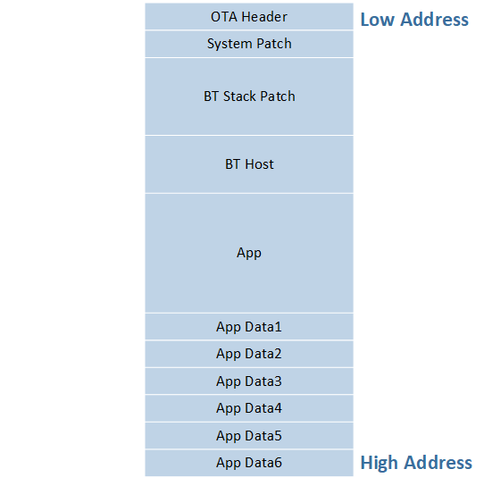
OTA Bank layout and description for each part is shown below.
Depending on different flash layouts, there are two OTA schemes: supporting Bank switching and non-support Bank switching.
Whether or not bank switching is supported, the boot patch image is always independently dual banked, serving the same function and acting as a backup
for each other.
For example, if the current boot patch is running in bank0, the OTA can only upgrade the boot patch in bank1.
After the upgrade is complete, the system will restart and choose the bank with the higher version number to run, if the version numbers are the same,
it will run in bank0.
The supporting bank switching scheme requires two identical OTA banks to back up each other.
The advantage of this scheme is that the program directly jumps to the new Bank to run, making the OTA upgrade switching process very fast after the
upgrade is completed and the system is rebooted.
The disadvantage is that it increases the flash overhead, so in general, when choosing the supporting bank switching scheme, the flash size should be
relatively large.
The Flash layout of the non-support bank switching scheme and the supporting bank switching scheme have the following differences.
The capacity of OTA Bank1 area is not allocated.
The OTA TMP area needs to be allocated, and its size should not be less than the largest image size in OTA Bank0. Therefore, the non-support bank switching scheme relatively saves flash space. After the OTA transmission is completed, the boot program will copy the data in the OTA TMP area to the specified image area in OTA Bank 0, and then restart to take effect, which relatively increases the restart time after the OTA upgrade is completed.
The non-support bank switching scheme also supports combined image upgrades, which is enabled by default. When using a combined image upgrade, when writing the image data to the OTA TMP area, it will calculate whether the remaining space in the OTA TMP area can accommodate the next image file that needs to be written. If it can, it will continue to write the next image file to the OTA temp area. When it can't, it will copy the data in the OTA TMP area to the OTA Bank0 area. The advantage of combined upgrading is to reduce the number of restarts and speed up the transmission rate.
Advantages: The total size of the bank is fixed. There is a backup bank, You can dynamically adjust the size of each image in the bank.
Disadvantages: The utilization rate of flash space is low.
Maintenance: It is necessary to maintain images for two bank corresponding addresses. The image released by Realtek by default only supports running on bank0. If you need to run on bank1, you need to contact Realtek to obtain it.
Advantages: The utilization rate of flash space is higher.
Disadvantages: Each image cannot be upgraded at the same time, and there are situations where old and new combinations coexist. After OTA is completed, activating the image will increase the boot time for that time.
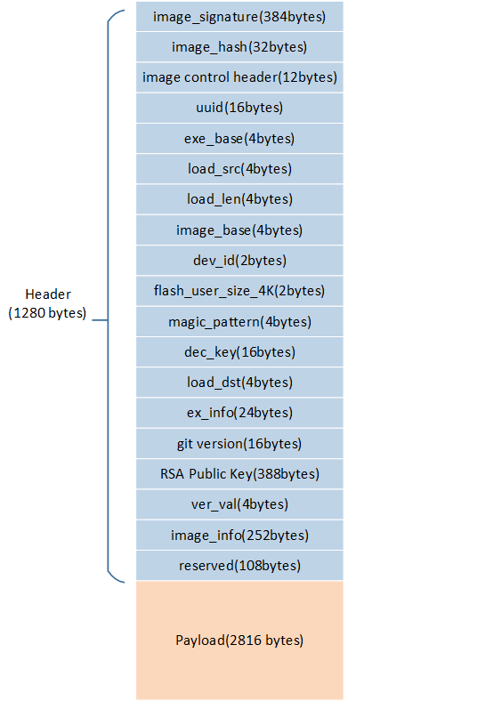
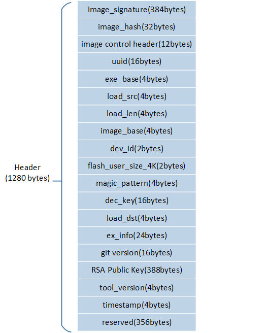
All images that support upgrades are composed of a 1280-Bytes image header and a variable-length payload. The image header contains the image type, size, version number, hash value, signature information, etc. The headers in the OTA Header file and other images are slightly different, which are explained below.
ctrl_header format in Image Header is shown as follows.
typedefstruct_IMG_CTRL_HEADER_FORMAT{uint16_tcrc16;uint8_tic_type;uint8_tsecure_version;union{uint16_tvalue;struct{uint16_txip:1;// payload is executed on flashuint16_tenc:1;// all the payload is encrypteduint16_tload_when_boot:1;// load image when bootuint16_tenc_load:1;// encrypt load part or notuint16_tenc_key_select:3;// referenced to ENC_KEY_SELECTuint16_tnot_ready:1;//for copy image in otauint16_tnot_obsolete:1;//for copy image in otauint16_tintegrity_check_en_in_boot:1;// enable image integrity check in boot flowuint16_tcompressed_not_ready:1;uint16_tcompressed_not_obsolete:1;uint16_trsvd:1;uint16_timage_type:3;/*for app 000b: normal image, 001b:compressed image, other for more types for patch in temp bank consist of 001b: patch+fsbl, 010b: patch+app, 011b: patch+fsbl+app*/};}ctrl_flag;uint16_timage_id;uint32_tpayload_len;}T_IMG_CTRL_HEADER_FORMAT;
ic_type represents IC type, which has the value of 15 when RTL87x2G chip is used.
secure_version indicates version of secure boot image.
image_id identifies different types of image, among which SCCD, OCCD cannot be updated through OTA.
typedefenum{IMG_SCCD=0x379D,IMG_OCCD=0x379E,IMG_BOOTPATCH=0x379F,/*!< KM4 boot patch */IMG_DFU_FIRST=IMG_BOOTPATCH,IMG_OTA=0x37A0,/*!< OTA header */IMG_SECUREMCUAPP=0x37A2,/*!< KM4 secure app */IMG_SECUREMCUAPPDATA=0x37A3,/*!< KM4 secure app data */IMG_BT_STACKPATCH=0x37A6,/*!< BT stack patch */IMG_BANK_FIRST=IMG_BT_STACKPATCH,IMG_MCUPATCH=0x37A7,/*!< KM4 non-secure rom patch */IMG_UPPERSTACK=0x37A8,/*!< KM4 non-secure Upperstack */IMG_MCUAPP=0x37A9,/*!< KM4 non-secure app */IMG_MCUCFGDATA=0x37AA,/*!< KM4 MCUConfigData */IMG_MCUAPPDATA1=0x37AE,IMG_MCUAPPDATA2=0x37AF,IMG_MCUAPPDATA3=0x37B0,IMG_MCUAPPDATA4=0x37B1,IMG_MCUAPPDATA5=0x37B2,IMG_MCUAPPDATA6=0x37B3,IMG_ZIGBEESTACK=0x37B4,/*!< KM4 Zigbee stack */IMG_MAX=0x37B5,IMG_DFU_MAX=IMG_MAX,IMG_RO_DATA1=0x3A81,IMG_RO_DATA2=0x3A82,IMG_RO_DATA3=0x3A83,IMG_RO_DATA4=0x3A84,IMG_RO_DATA5=0x3A85,IMG_RO_DATA6=0x3A86,IMG_USER_DATA8=0xFFF7,/*!< the image data only support unsafe single bank ota */IMG_USER_DATA_FIRST=IMG_USER_DATA8,IMG_USER_DATA7=0xFFF8,/*!< the image data only support unsafe single bank ota */IMG_USER_DATA6=0xFFF9,/*!< the image data only support unsafe single bank ota */IMG_USER_DATA5=0xFFFA,/*!< the image data only support unsafe single bank ota */IMG_USER_DATA4=0xFFFB,/*!< the image data only support unsafe single bank ota */IMG_USER_DATA3=0xFFFC,/*!< the image data only support unsafe single bank ota */IMG_USER_DATA2=0xFFFD,/*!< the image data only support unsafe single bank ota */IMG_USER_DATA1=0xFFFE,/*!< the image data only support unsafe single bank ota */IMG_USER_DATA_MAX=0xFFFF,/*!< the image data only support unsafe single bank ota */}IMG_ID;
备注
The unit of payload_len is bytes, which indicates the size of the image, not including the 1280 bytes of the image header. The total length of the image is the payload_len plus 1280 bytes.
crc16 represents performing crc and SHA256 verification on the image. The prepend_header tool will calculate crc and sha256 values at the same time, and SHA256 check is used by default.
The ctrl_flag and its bit-fields related to OTA are only not_ready and not_obsolete.
not_ready indicates whether the image is valid. By default, the not_ready field in the image header of files published, compiled, or generated by tools is all 0.
There is a risk of power outage when transferring the image to the backup area via Bluetooth. Therefore, before writing to the backup area, you need to change not_ready to 1 and then write to the flash.
Only when the image transfer is complete and the image integrity check is successful, modify the not_ready in the backup area image to 0, indicating the backup area image is valid.
After the system restarts, the activation process of the backup image is completed by the BootLoader.
not_obsolete indicates if the image should be abandoned and its default value is 1.
When bank switching is supported, not_obsolete is invalid during the OTA process.
When bank switching is not supported, after the OTA upgrade is complete, the boot code determines that not_ready is 0 and not_obsolete is 1. At this time, the image will be transferred from the OTA_TMP area to the corresponding image run area in OTA Bank0. After the transfer is successful, write the not_obsolete in the OTA_TMP area image to 0 to prevent repeated transfers. This ensures that the upgraded image is properly installed and run, and the old image is marked as obsolete to avoid being used again.
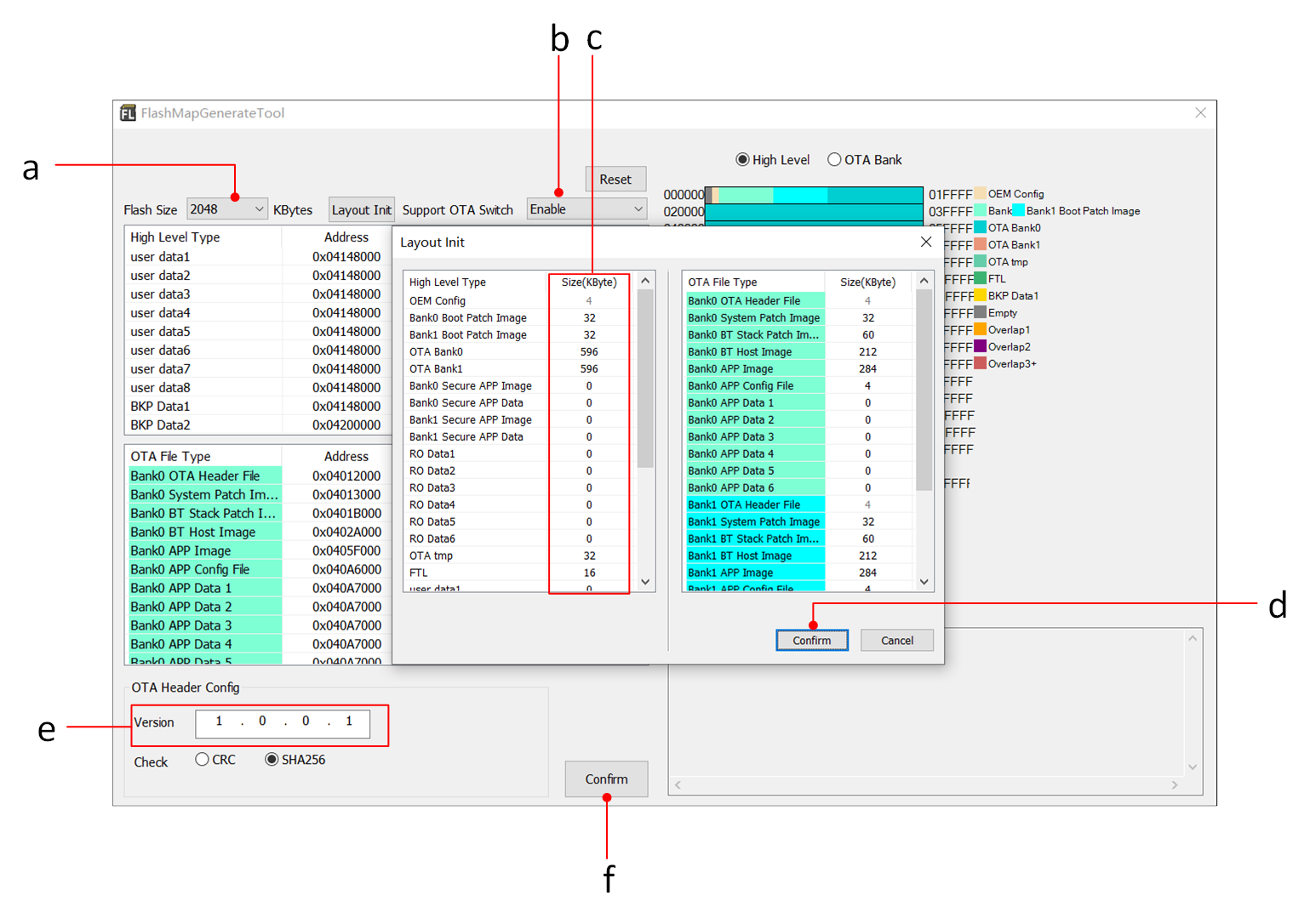
Generate flash_map.h, flashmap.ini and OTAHeaderfile.
备注
flash_map.h needs to be placed in the upper-level directory of the project to participate in the compilation and generate the APP image.
flashmap.ini is the input file of MPPackTool and MP Tool, and it is necessary to ensure that the image is consistent with all the output addresses set.
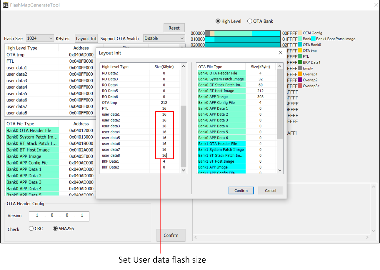
Use FlashMapGenerateTool to flashmap.ini, flash_map.h, Bank0OTAHeaderfile and Bank1OTAHeaderfile.
Select Flash Size.
Select Enable bank switch.
Set up two-level flash layout.
Click Confirm to complete the flash layout settings.
Modify OTA Header file version.
Click Confirm to generate flash_map.h, flashmap.ini, Bank0OTAHeaderfile and Bank1OTAHeaderfile.
Flash layout config and generate ota header image
备注
The version number of the OTA Header used for packaging is higher than the version number of the original running version, so that the new bank can take effect normally after the OTA upgrade.
Copy flash_map.h to the upper-level directory with project.
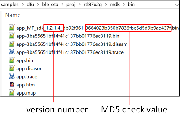
Link and compile the project to generate app_MP_sdk#####+version+MD5.bin file for packaging.
Supporting Bank switching scheme needs to compile the app images of OTA BANK0 and OTA BANK1. The demo app project in the Realtek released SDK can only compile the app image of OTA BANK0 by default. Compiling app image of OTA BANK1 need modify the macro ‘APP_BANK’ in mem_config.h in the upper-level directory as the project file to 1.
/** @brief set app bank to support OTA: 1 is ota bank1, 0 is ota bank0 */#define APP_BANK 1
Get system patch, stack patch and BT Host image that runs runs in OTA Bank1.
备注
The default released system patch, stack patch and BT host image can only run in OTA Bank0. Please consult Realtek to get system patch, stack patch and BT Host image that runs in OTA Bank1, when you choose bank switching method.
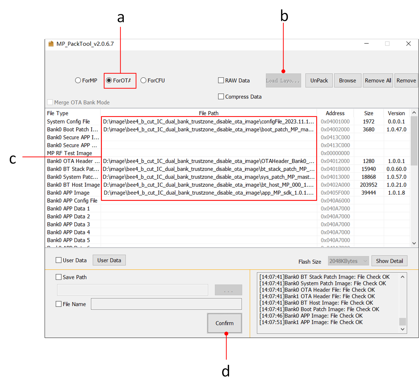
Generate packet file of ImgPacketFile-xxxxxx.bin in current directory, which is used for updating.
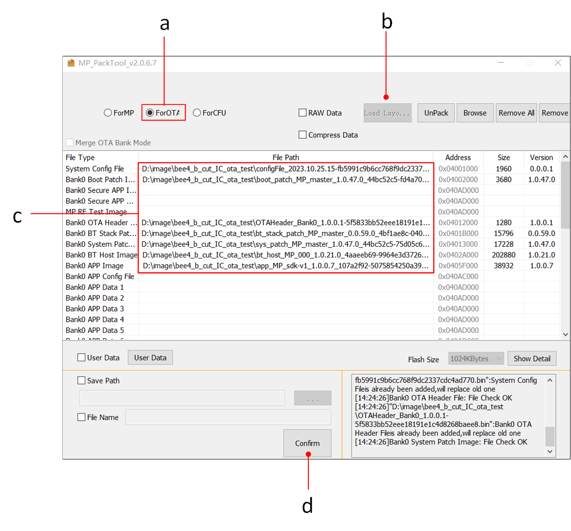
Select ForOTA option.
Load the generated flashmap.ini.
Load all OTA Bank0 and Bank1 images according to the set flash map.
Click Confirm to generate the package file.
Use the MPPackTool to package files -- supporting bank switching
备注
Both Bank0 OTA Header file and Bank1 OTA Header file need to be packaged, different from the scheme non-support bank switching.
All the contents defined in flash layout need to be packaged.
It is recommended that package both bank0 and bank1.
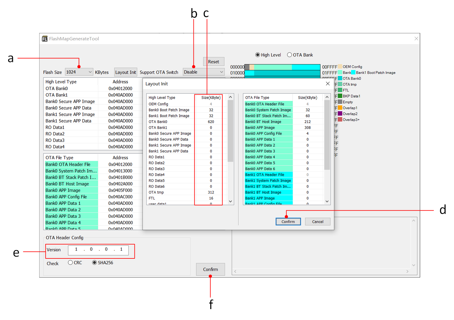
Use FlashMapGenerateTool to flashmap.ini, flash_map.h and Bank0OTAHeaderfile.
Select Flash Size.
Select Disable bank switch.
Set up two-level flash layout.
Click Confirm to complete the flash layout settings.
Modify OTA Header file version.
Click Confirm to generate flash_map.h, flashmap.ini and Bank0OTAHeaderfile.
Configure Flash Layout and generate Bank0 OTA Header file
备注
The flashmap.ini generated here needs to be consistent with the flashmap.ini used in the MP stage.
Copy flash_map.h to project directory. Link and compile the project to generate app_MP_sdk#####+version+MD5.bin file for packaging. To apply the non-support Bank switching scheme, mem_config.h in project directory should be modified.
/* @brief set app bank to support OTA: 1 is ota bank1, 0 is ota bank0 */#define APP_BANK 0
Open MP Pack Tool to load flash_map.ini generated in previous step and load corresponding image.
Select ForOTA option.
Load the generated flashmap.ini.
Load all OTA Bank0 images according to the set flash map.
Click Confirm to generate the package file.
Use the MPPackTool to package files -- non-support bank switching
备注
Bank0 OTA Header file can’t be packaged, which is different from the scheme supporting bank switching.
If only Patch Image or APP Image, either of them can be packaged.
Use Flash Map Generate Tool to flashmap.ini, flash_map.h and Bank0OTAHeaderfile.
Configure Flash Layout and generate Bank0 OTA Header file
备注
The flashmap.ini generated here needs to be consistent with the flashmap.ini used in the MP stage.
Copy flash_map.h to project directory and open the project with Keil. Link and compile the project to generateapp_MP_sdk#####+version+MD5.bin file for packaging.
Use the script in SDK/tools/UserData to generate a User Data file that supports packaging.
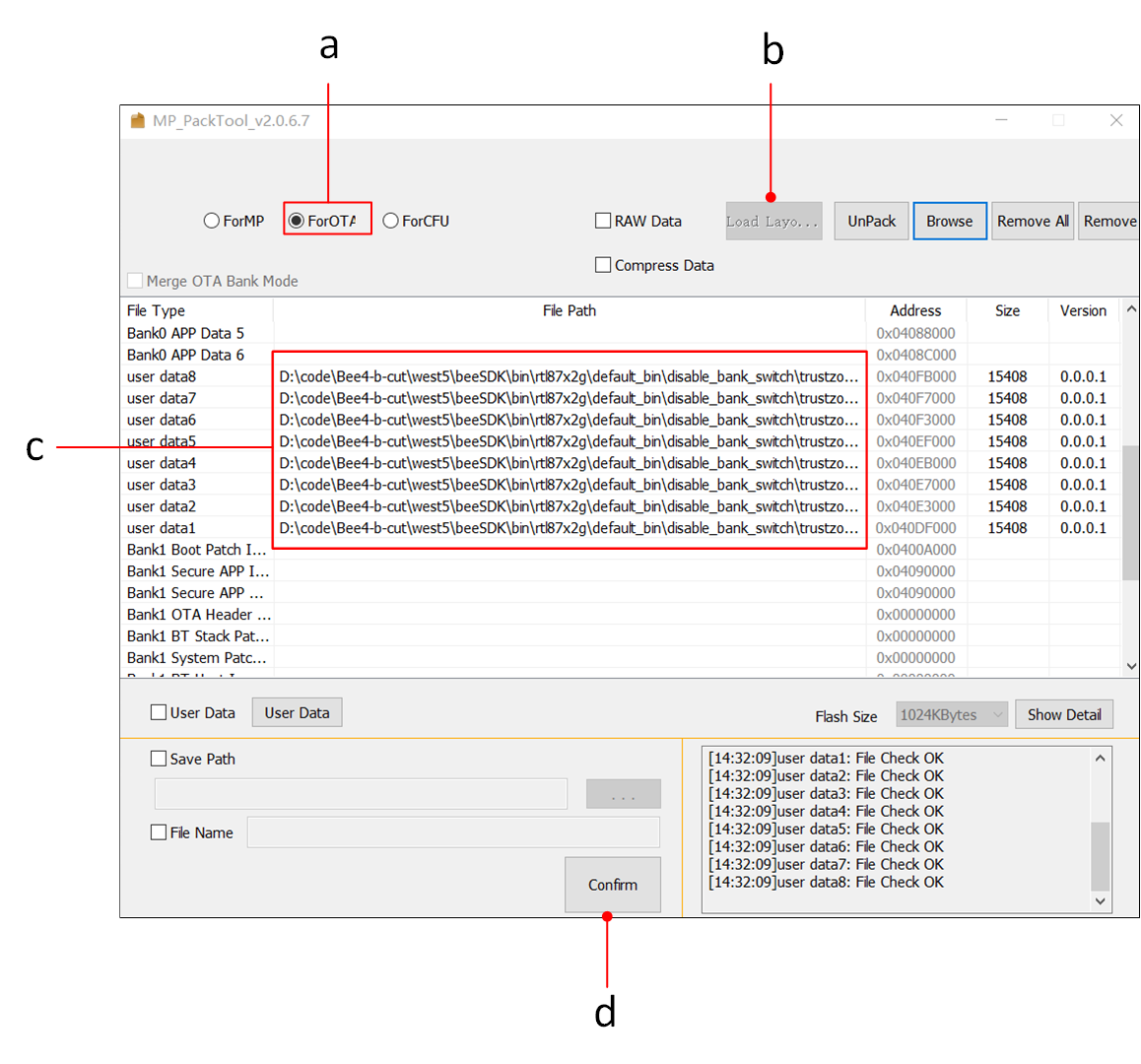
Open MPPackTool to load flash_map.ini generated in previous step and load corresponding image.
Select ForOTA option.
Load the generated flashmap.ini.
Load User data image according to the set flash map.
Click Confirm to generate the package file.
Use the MPPackTool to package files – User Data upgrade
备注
If you only need to update a certain User Data, you can package only one of them.
Allows User Data to be packaged and upgraded together with other images.
OTA is divided into silent OTA and normal OTA depending on the transmission protocol.
Silent OTA
During the image upgrade process, the original functions of the device can be used normally. After the upgrade is completed, it only takes a short restart time for the program to automatically switch to the new functions.
Normal OTA
The function is stable. However, the upgrade process requires switching the device to DFU mode, and the original functions cannot be used until the upgrade is completed.
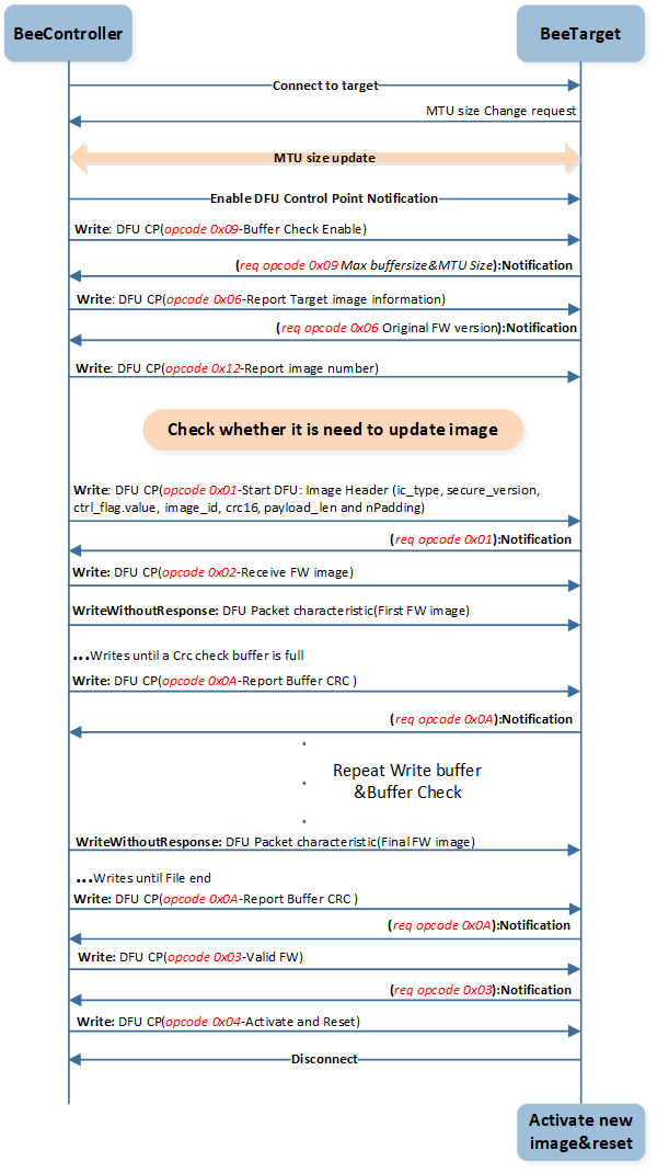
Both types of upgrades will use the OTA Service and DFU Service.
The OTA Service is used to obtain device information or enter DFU mode, while the DFU Service is used to execute the upgrade process.
After receiving the ctrl header of image, it needs to be decrypted and then parsed, not_ready will be temporarily written to 1 and then written to flash.
During data transmission, if AES encryption is supported, every 16 bytes is encrypted. After the receiving end receives the data, it needs to be decrypted first. The last part less than 16 bytes is sent without encryption. When the buffer check size is full, write to flash.
Without bank switching, when the packaged file to be upgraded contains Patch, APP or APP DATA, one file upgrade needs to be successfully verified. After the copy is restarted and activated to take effect, the next file can be upgraded.
Without bank switching with supports combined image upgrades, when writing image data to the OTA temporary area, it calculates whether the remaining space in the OTA TMP area can accommodate the next image file to be written. If it can, it continues to write the next image file to the OTA TMP area. When it cannot, it moves the data in the OTA TMP area to the OTA Bank0 area. After restarting, copying, and activating, it upgrades other files.
With bank switching, the program cannot be rebooted until all the files have been updated and verified when the packaged file includes OTA Header, Patch, APP or APPDATA. Otherwise, this update will be invalid for that all the files in bank region must come into effect to ensure the program is running properly with bank switching.