OTA (Over-The-Air) technology refers to a method of remotely updating the flash storage of RTL87x2G series devices via Bluetooth transmission. This technology provides an efficient and convenient way for devices to receive and install updates without the need for physical connections or manual intervention. The SDK supports OTA functionality wirelessly, making it compatible with devices running Android and iOS systems. Specifically, the SDK utilizes the GATT (Generic Attribute Profile) protocol for Bluetooth data transmission to ensure the stability and reliability of the update process. Moreover, OTA updates can not only enhance the performance and functionality of the devices but also fix known vulnerabilities and security issues, thereby improving user experience and device security.
Depending on different Flash Layout, there are two OTA schemes:
Supporting Bank Switching Scheme
OTA Bank0 and OTA Bank1 will serve as backup firmware storage areas for each other. During firmware updates, these two storage areas can be used interchangeably, ensuring that the system can roll back to the previous backup firmware in case of a failed update, thereby guaranteeing system stability and security.
Non-Supporting Bank Switching Scheme
OTA Bank1 does not need to be allocated space. Instead, the OTA TMP area needs to be allocated, and its size must be no less than the largest image size of OTA Bank0, thereby saving Flash space relatively. Once the OTA transmission is complete, the BootLoader will move the data from the OTA TMP area to the designated image area of OTA Bank0, and then reboot to apply the update, which relatively increases the reboot time required to complete the OTA upgrade.
Note
The supporting Bank switching OTA scheme requires maintaining images for both Bank addresses. The image released by default by Realtek only supports running on Bank0, if user need to run it on Bank1, please contact Realtek for assistance.
Whether or not Bank switching is supported, the Boot Patch image is always independently dual-banked, serving the same function and acting as a backup for each other. For example, if the current Boot Patch is running in Bank0, the OTA can only upgrade the Boot Patch in Bank1. After the upgrade is complete, the system will restart and choose the Bank with the higher version number to run. If the version numbers are the same, it will run in Bank0.
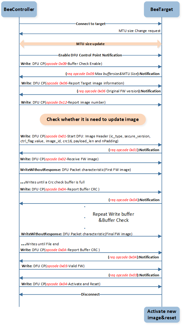
The OTA upgrade process is as follows. The overall process of the OTA update and the interaction between the various modules can be more clearly understood from the diagram. In this process, the mobile phone acts as the Controller, and the SoC as the Target. Before the OTA begins, the Controller and Target establish a connection. Subsequently, the Controller retrieves information from the Target to determine whether an upgrade is permissible.
OTA upgrades can be categorized into Silent OTA and Normal OTA based on different transmission protocols.
Silent OTA
During the image upgrade process, the original functions of the device can be used normally. After the upgrade is completed, it only takes a short restart time for the program to automatically switch to the new functions.
Normal OTA
The function is stable. However, the upgrade process requires switching the device to DFU mode, and the original functions cannot be used until the upgrade is completed.
Note
Both types of upgrades will use the OTA Service and DFU Service.
OTA Service: used to obtain device information or enter DFU mode.
After receiving the image control header, the not_ready in the image control header is temporarily set to 1 and then written into the flash. Once the image transfer is completed and the image integrity check is successful, the not_ready in the backup area image is changed to 0 to mark the backup area image as valid. This design ensures that when the OTA transfer is interrupted, the BootLoader can easily identify whether the image is in a ready state.
During data transmission, if AES encryption is used, every 16 bytes of data will be encrypted, and the part less than 16 bytes will not be encrypted and sent directly. After receiving the data, the receiving end needs to decrypt the encrypted part first.
If buffer check is enabled, data is written into the flash after the buffer check size is fully received.
During an OTA upgrade, the upgrade image is transmitted to the upgrade area via the OTA Service and DFU Service. Once the transfer is complete, a reboot occurs and the Bootloader handles the activation process.
While writing the image data to the OTA TMP area, the remaining space in the OTA TMP area will be calculated to determine if it can accommodate the next image file to be written. If it can, the process continues by writing the next image file to the OTA TMP area. If it cannot, the data in the OTA TMP area is moved to the OTA Bank0 region, and after a restart, the copy and activation take effect. Subsequently, the next file can be upgraded.
Non-Supporting Combined Image Upgrades
When the packaged file to be upgraded contains Patch, APP, or APP DATA, one file upgrade needs to be successfully verified. After the copy is restarted and activated to take effect, the next file can be upgraded.
When the packaged files to be upgraded contain OTA Header file, Patch, APP, or APP DATA, each file must be individually transmitted and validated as successfully received before transmitting and validating the next file. All files must be successfully transmitted and validated before a reboot can occur, otherwise, the current upgrade attempt will be invalid. This is because, in the bank switching scheme, all files in the Bank area need to become effective together for the system to run properly.
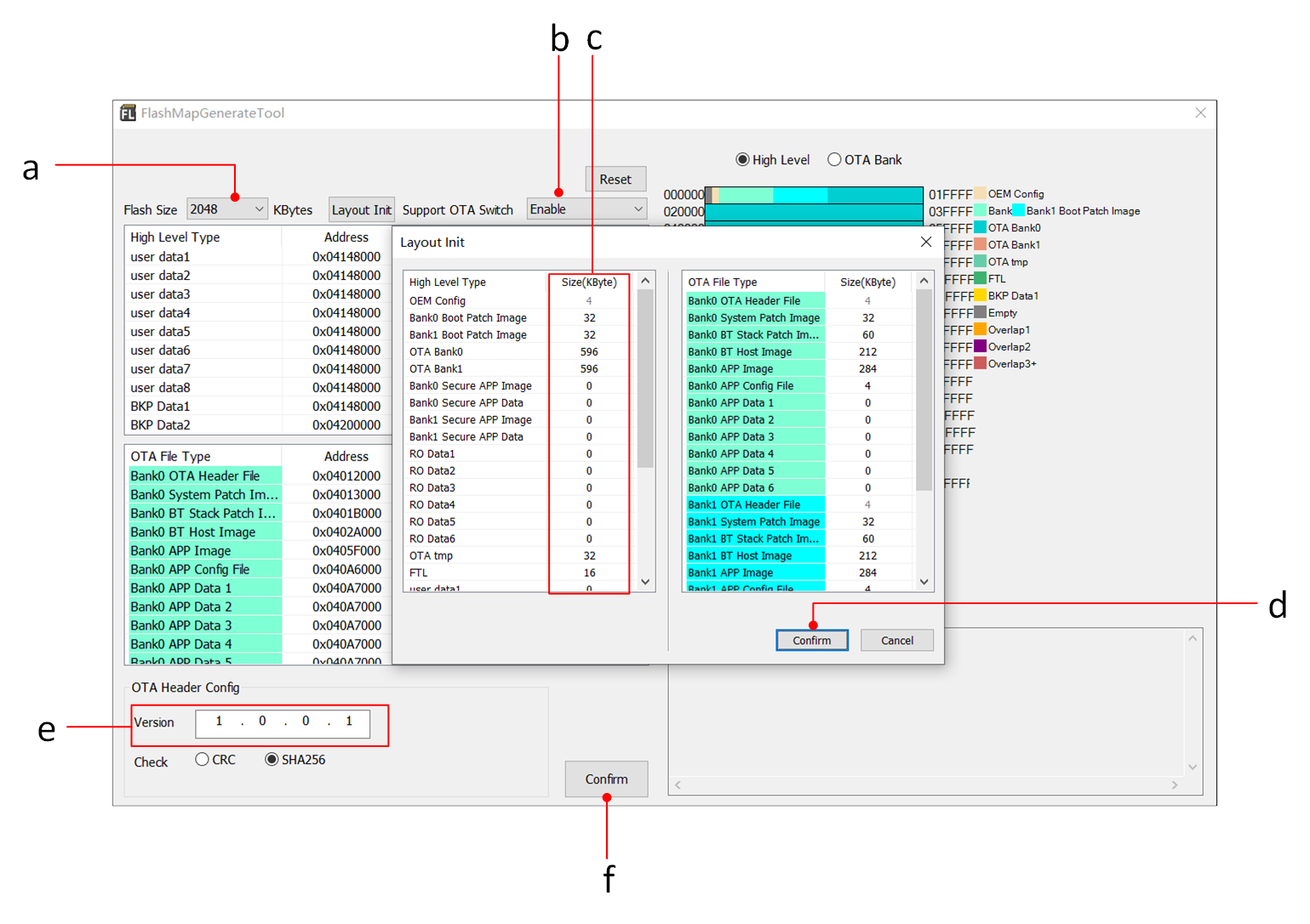
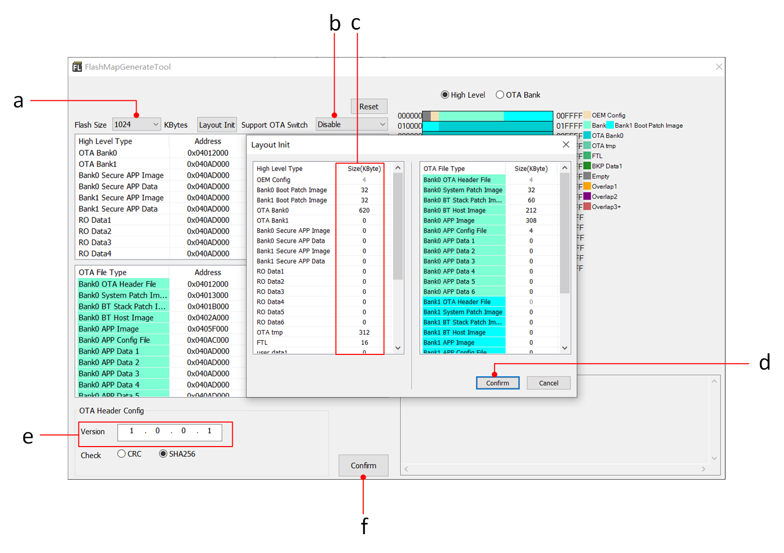
Use Flash Map Generate Tool to flashmap.ini, flash_map.h, Bank0OTAHeaderfile and Bank1OTAHeaderfile.
Flash Size select an appropriate size.
Support OTA Switch select Enable.
Set up two-level flash layout.
Click Confirm to complete the flash layout settings.
Modify the OTA Header file version at Version.
Click Confirm to generate flash_map.h, flashmap.ini, Bank0OTAHeaderfile and Bank1OTAHeaderfile.
Flash Layout Config and Generate OTA Header - Supporting Bank Switching
Note
The version number of the OTA Header used for packaging is higher than the version number of the original running version, so that the new bank can take effect normally after the OTA upgrade.
Copy flash_map.h to the upper-level directory with the project.
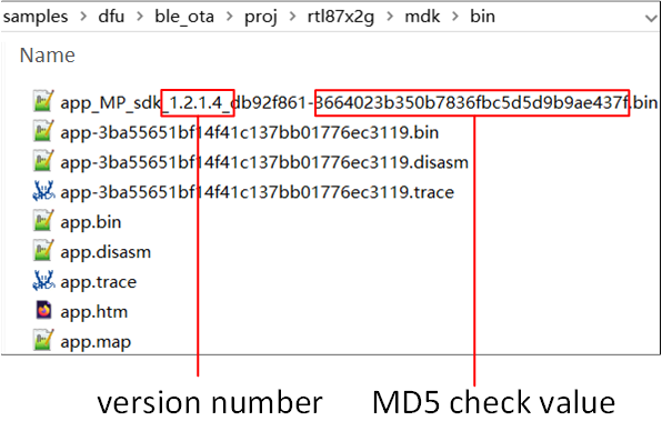
Link and compile the project to generate app_MP_sdk#####+version+MD5.bin file for packaging.
Supporting Bank switching scheme needs to compile the app images of OTA Bank0 and OTA Bank1.
The demo APP project in the Realtek released SDK can only compile the app image of OTA Bank0 by default. Compiling app image of OTA Bank1 needs modifying the macro #defineAPP_BANK in mem_config.h in the upper-level directory as the project file to 1.
/** @brief set app bank to support OTA: 1 is ota bank1, 0 is ota bank0 */#define APP_BANK 1
Get the System Patch, BT Stack Patch, and BT Host image that runs in OTA Bank1.
Note
The default released System Patch, BT Stack Patch, and BT host image can only run in OTA Bank0. Please consult Realtek to get the System Patch, BT Stack Patch, and BT Host image that runs in OTA Bank1 when choosing the supporting Bank switching scheme.
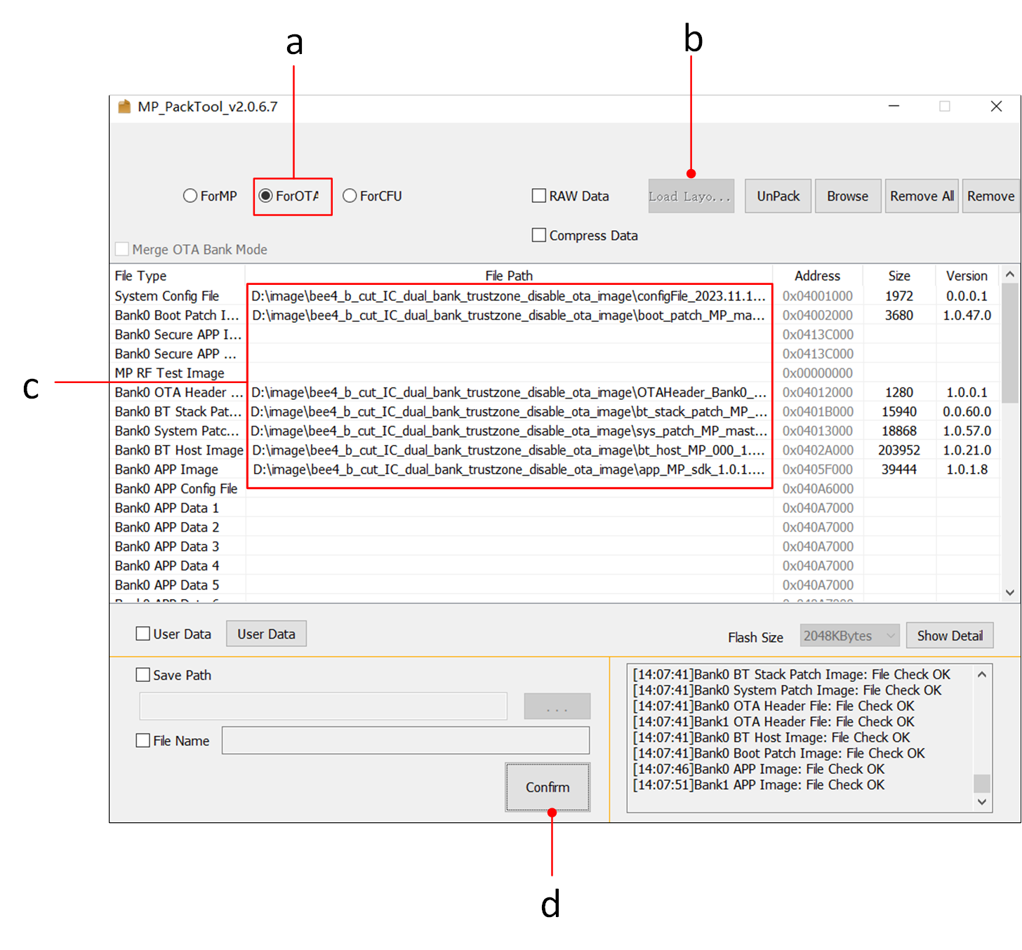
Generate a packet file of ImgPacketFile-xxxxxx.bin in the current directory, which is used for updating.
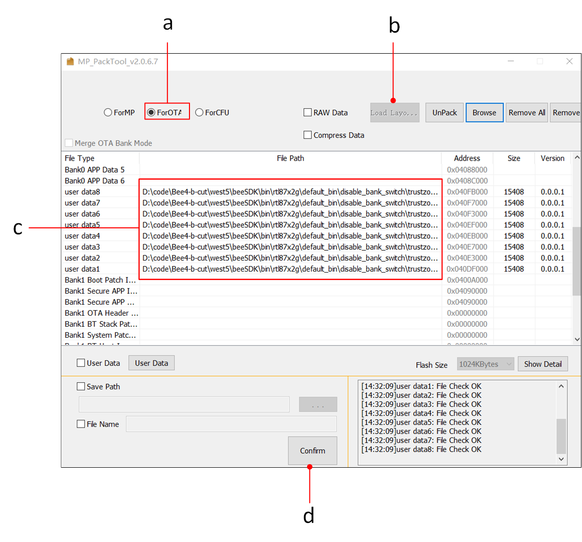
Select the ForOTA option.
Load the generated flashmap.ini.
Click Browse to load all OTA Bank0 and Bank1 images.
Use Flash Map Generate Tool to flashmap.ini, flash_map.h, and Bank0OTAHeaderfile.
Flash Size select an appropriate size.
Support OTA Switch select Disable.
Set up two-level flash layout.
Click Confirm to complete the flash layout settings.
Modify the OTA Header file version at Version.
Click Confirm to generate flash_map.h, flashmap.ini, and Bank0OTAHeaderfile.
Flash Layout Config and Generate OTA Header - Non-supporting Bank Switching
Note
The flashmap.ini generated here needs to be consistent with the flashmap.ini used internally within the SoC.
Copy flash_map.h to the project directory. Link and compile the project to generate app_MP_sdk#####+version+MD5.bin file for packaging.
Note
Non-supporting Bank switching scheme only needs to compile the OTA Bank0 image. The configuration can be found in the project's parent directory in the mem_config.h file under #defineAPP_BANK. The specific code is as follows:
/* @brief set app bank to support OTA: 1 is ota bank1, 0 is ota bank0 */#define APP_BANK 0
Generate a packet file of ImgPacketFile-xxxxxx.bin in the current directory, which is used for updating.
APP Data Tool is used to convert the original APP Data bin file into an APP Data type image that can be programmed into Flash using the MP Tool.
After processing with the APP Data Tool, a 512-byte MP header and a 1280-byte image header will be added to the original APP data. These headers are used for MP Tool programming and Bootloader verification, respectively. Suppose the original APP Data bin file size is 120KB. The final size programmed into the flash will be 1280 bytes of the image header plus 120KB of the APP data payload.
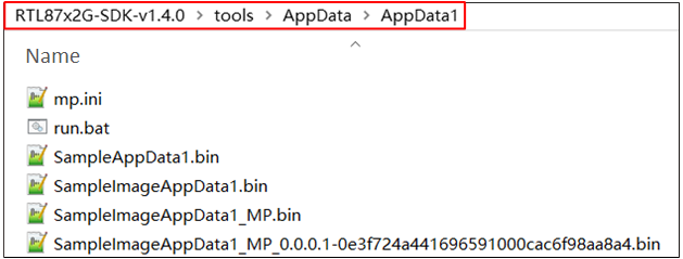
The following example uses APP Data1, with the specific path as follows:
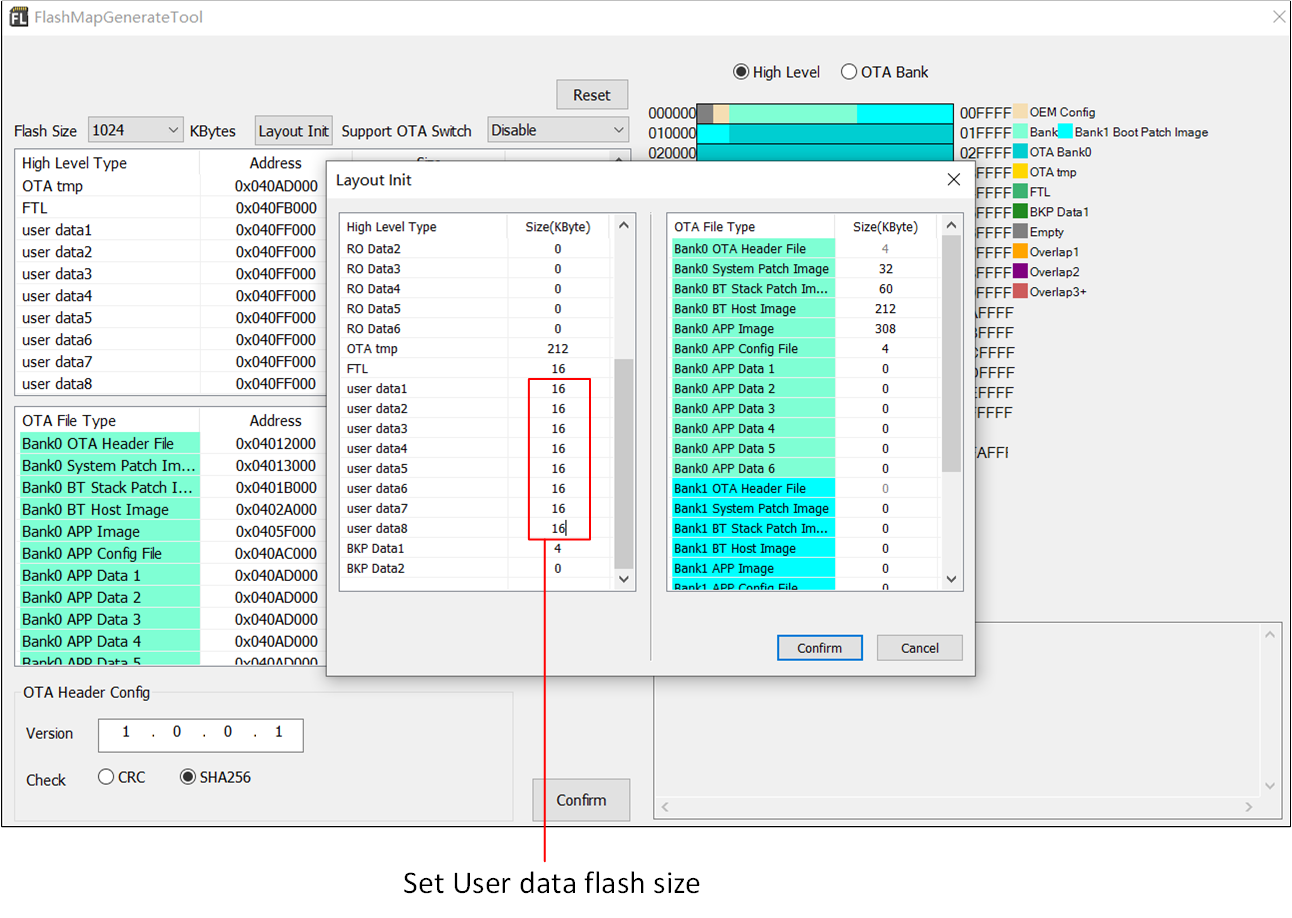
User Data is primarily used to store data that does not affect system functionality. The upgrade strategy for User Data differs from other images. For other images, they are first transferred to the OTA TMP area, while User Data is directly transferred to its corresponding Flash address.
Below is an example of upgrading User Data with a 1M byte flash. The flash layout is shown in the table below: