Flash
Flash is not the same as RAM since it is non-volatile storage. RAM enables direct access to read and write data. However, if flash is not empty, an erase operation is typically required before performing a flash write operation.
备注
Generally, flash has a maximum of 100,000 programming cycle limit, and if a block is frequently erased and written, it is prone to becoming a bad block. Flash driver is not preferred to be used by application layer, while FTL is suggested.
Flash Layout
The RTL87x2G chip integrates a flexible memory controller (FMC) that supports external SPI Flash. The FMC supports a maximum address mapping space of 64M bytes, corresponding to the address space 0x04000000 ~ 0x07FFFFFF.
The flash layout is set in two levels, including the High-Level Flash map and the OTA Bank map. For methods on adjusting the flash layout, refer to Method of Adjusting Flash layout.
High Level Flash Map
In the RTL87x2G SDK, the High Level Flash Map is composed of 11 parts, including Reserved, OEM Header (the storage space of the config file), Bank0 Boot Patch, Bank1 Boot Patch, OTA Bank 0, OTA Bank 1, Bank0 Secure APP (optional), Bank1 Secure APP (optional), OTA Tmp, FTL and APP Defined Section, such as High Level Flash Map shows.
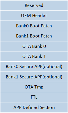
High Level Flash Map
The function introduction of each part in the flash layout is shown below.
Memory Segment |
Starting Address |
Size( Bytes) |
Functions |
|---|---|---|---|
Reserved |
0x04000000 |
0x1000 |
Reserved |
OEM Header |
0x04010000 |
0x1000 |
Stores configuration information which includes BT Address, AES Key and user defined Flash layout. |
Bank0 Boot Patch |
Variable (Determined by eFuse) |
Variable (Determined by eFuse) |
Flash boot loader, Bank0 Boot Patch and Bank1 Boot Patch have the same function and serve as backup areas for each other. |
Bank1 Boot Patch |
Variable (Determined by eFuse) |
Variable (Determined by eFuse) |
Flash boot loader. |
OTA Bank0 |
Variable (Determined by eFuse) |
Variable (Determined by eFuse) |
Store data and code running area, further subdivided into OTA Header, System Patch, BT Stack Patch, BT Host, APP, APP Data1, APP Data2, APP Data3, APP Data4, APP Data5, APP Data6. If you choose the OTA solution that does not switch banks, the OTA_TMP area is used as the Ota backup area; on the contrary, if you choose the OTA solution that switches banks, OTA bank0 and OTA bank1 have the same function and serve as backup areas for each other. |
OTA Bank1 |
Variable (Determined by eFuse) |
Variable (Determined by eFuse) |
The same as bank0, and the size of bank1 must also be the same with bank0. |
Bank0 Secure APP |
Variable (Determined by eFuse) |
Variable (Determined by eFuse) |
It is only required under TrustZone enable. Trustzone is enabled in Secure APP. Bank0 Secure APP and Bank1 Secure APP have the same function and serve as backup areas for each other. |
Bank1 Secure APP |
Variable (Determined by eFuse) |
Variable (Determined by eFuse) |
It is only required under TrustZone enable. |
OTA TMP |
Variable (Determined by eFuse) |
Variable (Determined by eFuse) |
When using non-support OTA bank switching scheme, this area is used as a backup for OTA images. Its size cannot be smaller than the size of the app image area in OTA bank0. |
FTL |
Variable (Determined by eFuse) |
Variable (Determined by eFuse) |
Support accessing flash with logic address. User can read/write flash with unit size of 4 bytes at least. |
APP Defined Section |
Variable (Determined by eFuse) |
Variable (Determined by eFuse) |
The remaining zone of the flash. User can use it freely except for OTA update. |
OTA Bank Map
In the RTL87x2G SDK, the OTA Bank includes 12 types of images, namely OTA Header,System Patch,BT Stack Patch, BT Host, APP, APP Config File, APP Data1, APP Data2, APP Data3, APP Data4, APP Data5, APP Data6, the description of each part is shown in OTA Bank layout, and the description of each part in the layout is shown in Image Description of OTA Bank. The layout of the OTA Bank level is determined by the OTA header. OTA headers with different OTA Bank layouts can be generated through FlashMapGenerateTool.
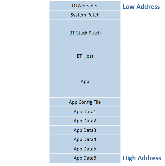
OTA Bank layout
MemorySegment |
Starting Address |
Size |
Functions |
|---|---|---|---|
OTA Header |
Depend by OEM header |
4KB |
OTA version, start address and size of each bank. |
System Patch |
Depend by OTA header |
changeable |
Optimized and expanded code for systems in non-secure rom. |
BT Stack Patch |
Depend by OTA header |
changeable |
Bluetooth controller protocol stack optimization and extension code. |
BT Host |
Depend by OTA header |
changeable |
Implement part of the code of HCI and above Bluetooth protocol stack. |
APP |
Depend by OTA header |
changeable |
Running code for development solutions. |
App Config File |
Depend by OTA header |
changeable |
App Config information |
App Data1 |
Depend by OTA header |
changeable |
APP Data need to be updated by OTA. |
App Data2 |
Depend by OTA header |
chan geable |
APP Data need to be updated by OTA. |
App Data3 |
Depend by OTA header |
changeable |
APP Data need to be updated by OTA. |
App Data4 |
Depend by OTA header |
changeable |
APP Data need to be updated by OTA. |
App Data5 |
Depend by OTA header |
changeable |
APP Data need to be updated by OTA. |
App Data6 |
Depend by OTA header |
changeable |
APP Data need to be updated by OTA. |
Method of Adjusting Flash layout
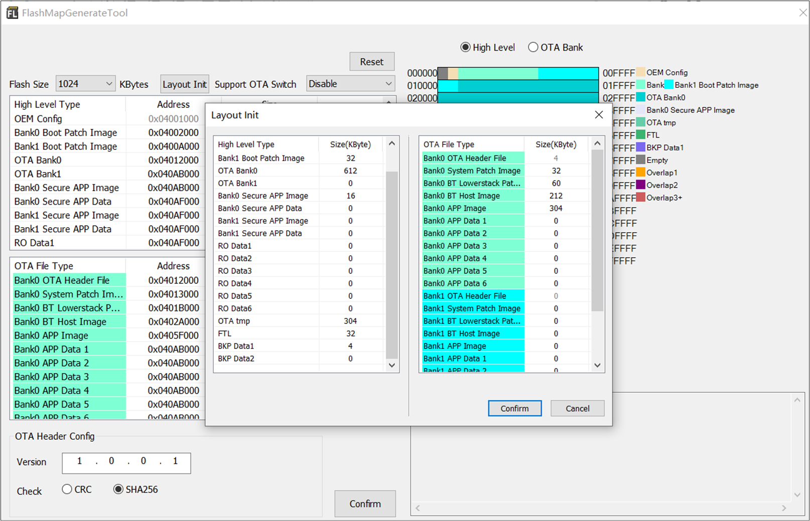
Flash layout settings are divided into two levels: the High Level Flash map is determined by the config file, while the OTA Bank map is determined by the OTA Header file. Users can configure custom flash layout through the Config Set option in MPTool, as shown below.
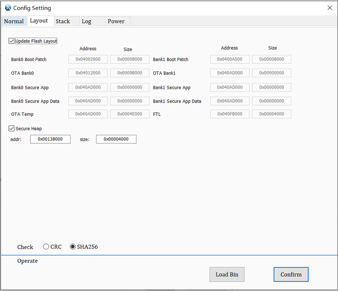
Generate config file through MPTool
For the convenience of users, Realtek also provides FlashMapGenerateTool for generating flash map.ini and 和 flash_map.h files. The flash map.ini file can be imported into MPTool to generate config file and OTA header respectively. The flash_map.h file needs to be copied to the APP project directory to compile a correct and runnable APP image.
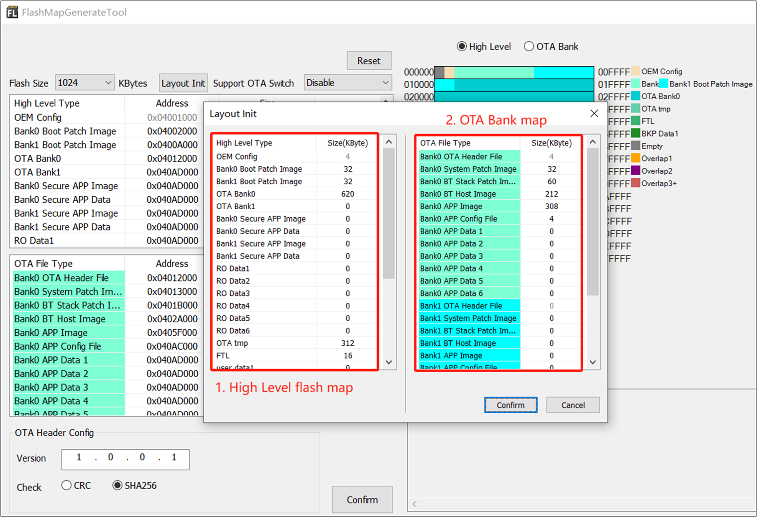
FlashMapGenerateTool configures Flash Map
But at the same time, the following principles must be followed to adjust the flash layout.
If you choose an OTA solution that supports bank switching, ensure that the size of OTA bank0 is equal to the size of OTA bank1, and set the size of the OTA TMP area to 0.
If you choose an OTA solution that supports bank switching, you can use different OTA bank layouts to generate the Bank0 OTA Header file and the Bank1 OTA Header file, but the sizes of OTA bank0 and bank1 must remain unchanged and not be smaller than the total size of the images within the OTA bank.
If you choose an OTA solution that does not support bank switching, set the size of OTA bank1 to 0, and the size of the OTA TMP area should not be smaller than the size of the largest image in OTA bank0.
The original APP Data bin file needs to be processed by the App Data tool provided in the RTL87x2G SDK before it can be burned by MPTool and packaged by MPPackTool. The tool path is in sdk/tools/AppData, and a 1280Byte image header that satisfies a specific format will be added after processing. If the data does not need to be upgraded, it should be placed in the "APP Defined Section" area.
In order to lock all the code areas to prevent unexpected flash write and erase operations, align the offset of the end address of OTA Bank1 relative to the start address of the flash to the actually selected flash address as much as possible. The range corresponding to a certain protection level supported, such as 64KB, 128KB, 256KB, 512KB, etc.
Because the data stored in the APP Data1, APP Data2, APP Data3, APP Data4, APP Data5 or APP Data6 area in the OTA bank may fall within the locked range of the flash, so this area is generally stored as read-only The data. If you need to store data that needs to be rewritten, it should be placed in the "APP Defined Section" area.
Flash Layout Example
Based on the above-mentioned rules for adjusting the flash layout, this section provides examples of the flash layout under without bank switch and supporting bank switch method.
Sample Flash Layout of OTA without Bank Switch
Example layout with a total flash size of 1MB |
Size(byte) |
Start Address |
|---|---|---|
Reserved |
4K |
0x04000000 |
OEM Header |
4K |
0x04001000 |
Bank0 Boot Patch |
32K |
0x04002000 |
Bank1 Boot Patch |
32K |
0x0400A000 |
OTA Bank0 |
612K |
0x04012000 |
|
4K |
0x04012000 |
|
32K |
0x04013000 |
|
60K |
0x0401B000 |
|
212K |
0x0402A000 |
|
304K |
0x0405F000 |
|
4K |
0x040AC000 |
|
0K |
0x040AD000 |
|
0K |
0x040AD000 |
|
0K |
0x040AD000 |
|
0K |
0x040AD000 |
|
0K |
0x040AD000 |
|
0K |
0x040AD000 |
OTA Bank1(equal to 0) |
0K |
0x040AD000 |
Bank0 Secure APP code |
0K |
0x040AD000 |
Bank0 Secure APP Data |
0K |
0x040AD000 |
Bank1 Secure APP code |
0K |
0x040AD000 |
Bank1 Secure APP Data |
0K |
0x040AD000 |
OTA Temp |
312K |
0x040AD000 |
FTL |
16K |
0x040FB000 |
APP Defined Section |
4K |
0x040FF000 |
Sample Flash Layout of OTA support Bank Switch
Example layout with a total flash size of 2MB |
Size(byte) |
Start Address |
|---|---|---|
Reserved |
4K |
0x04000000 |
OEM Header |
4K |
0x04001000 |
Bank0 Boot Patch |
32K |
0x04002000 |
Bank1 Boot Patch |
32K |
0x0400A000 |
OTA Bank0 |
596K |
0x04012000 |
|
4K |
0x04012000 |
|
32K |
0x04013000 |
|
60K |
0x0401B000 |
|
212K |
0x0402A000 |
|
284K |
0x0405F000 |
|
4K |
0x040A6000 |
|
0K |
0x040A7000 |
|
0K |
0x040A7000 |
|
0K |
0x040A7000 |
|
0K |
0x040A7000 |
|
0K |
0x040A7000 |
|
0K |
0x040A7000 |
OTA Bank1 |
596K |
0x040A7000 |
|
4K |
0x040A7000 |
|
32K |
0x040A8000 |
|
60K |
0x040B0000 |
|
212K |
0x040BF000 |
|
284K |
0x040F4000 |
|
4K |
0x0413B000 |
|
0K |
0x0413C000 |
|
0K |
0x0413C000 |
|
0K |
0x0413C000 |
|
0K |
0x0413C000 |
|
0K |
0x0413C000 |
|
0K |
0x0413C000 |
Bank0 Secure APP code |
0K |
0x0413C000 |
Bank0 Secure APP Data |
0K |
0x0413C000 |
Bank1 Secure APP code |
0K |
0x0413C000 |
Bank1 Secure APP Data |
0K |
0x0413C000 |
OTA Temp |
32K |
0x0413C000 |
FTL |
16K |
0x04148000 |
APP Defined Section |
736K |
0x040FF000 |
FTL
FTL (Flash Translation Layer) is a software abstraction layer built on the flash Driver, used for user read and write operations on flash data. The physical space location of FTL can be viewed at flash layout. The purpose of FTL is to simplify the process of modifying data in the flash:
Without FTL, modifying data on the flash requires the user to erase the flash first. When data is frequently modified, a significant amount of time is wasted on erasing. FTL, however, uses logical addresses instead of physical addresses to access the flash. When modifying data, the original data is not directly altered; instead, the new data is written to a new physical address, and the logical address points to this new physical address. This method avoids frequent flash erasures, saving time required for data modification.
When FTL detects that there is not enough space to write new records, it triggers the Garbage Collection (GC) mechanism to erase and reclaim outdated or unused records. By cyclically utilizing flash space and evenly distributing erase/write operations, FTL prevents certain blocks from failing prematurely, achieving wear leveling.
Currently, FTL supports both v1 and v2 versions. The v1 version includes a full implementation of the aforementioned features. Building upon v1, the v2 version improves maximum storage capacity and flash utilization, and supports creating logical space through "module" partitioning.
备注
FTL is suitable for data that needs frequent rewriting. On one hand, the API interface is simpler, and on the other hand, it helps to extend the lifespan of the flash (wear leveling).
If the data volume is large, read-only (or occasionally rewritten), and does not require OTA upgrade support, it is recommended to use the flash API to store data in the "APP Defined Section" area.
If the data volume is large, read-only (or occasionally rewritten), and requires OTA upgrade support, it is recommended to store data in the App Data1, App Data2, App Data3, App Data4, App Data5, App Data6, and secure app data areas within the OTA bank.
FTL v1
SDK V1.2.0 and previous versions support FTL v1 by default.If FTL v1 is needed in subsequent SDK versions, please follow these steps:
Open the SDK root directory.
Copy
ftl_v1\ftl.htobsp\sdk_lib\inc\, replacing the existingftl.hin the target path.If using GCC for compilation, copy
ftl_v1\librtl87x2g_sdk.atobsp\sdk_lib\lib\rtl87x2g\gcc, replacing the existinglibrtl87x2g_sdk.ain the target path.If using MDK for compilation, copy
ftl_v1\rtl87x2g_sdk.libtobsp\sdk_lib\lib\rtl87x2g\mdk, replacing the existingrtl87x2g_sdk.libin the target path.Recompile the APP project.
Functional Division of FTL Space
Currently, the FTL space is divided into the following two storage spaces according to its functions. Take the default FTL physical space size of 16K as an example.
BT storage space
Logic address range: [0x0000, 0x0D00). But this space size can be changed by otp parameter. (Currently not supported by SDK)
This region is used to store BT information such as device address, link key, etc.
Refer to LE Host for more details.
APP storage space
Logic address range: [0x0D00, 0x17F0).
APP can use this region to store user defined information.
The following APIs can be used to read/write APP storage data.
uint32_t ftl_save(void *pdata, uint16_t offset, uint16_t size);
uint32_t ftl_load(void *pdata, uint16_t offset, uint16_t size);
备注
When calling ftl_save or ftl_load, the bottom layer has encapsulated an offset, which is 0x0D00 by default.
Adjust the size of the FTL space
The physical space size of FTL is configurable, adjusted by modifying the configuration parameters in the config file (for more content related to flash layout adjustments, see: please refer to). The steps are as follows:
First, use FlashMapGenerateTool (released with MPTool) to generate
flash map.iniandflash_map.hfile.Copy the
flash_map.hfile to the APP project directory, for example:sdk\samples\bluetooth\ble_peripheral, so that the APP can obtain the correct loading address when compiling.Load
flash map.iniinto MPTool to generate config file for download. As shown in Modify the flash map configuration file, the physical space of FTL will be adjusted to 32K.
Modify the flash map configuration file
备注
When you adjust the size of the FTL physical space, the logical space available for the APP will also change accordingly. Assuming that the physical space size of the actual FTL is set to mK (m is an integer multiple of 4), the logical space available for the corresponding APP is equal to ((511*(m-4)-4)-3328) bytes.
In addition, in order to improve the efficiency of FTL reading, the bottom layer has made a mapping mechanism of physical address and logical address. This mapping table will occupy a certain amount of RAM space. When the FTL physical space size is set to 16K by default, this mapping table occupies 2298 bytes of buffer ram heap space. Suppose the physical space size of the actual FTL is set to mK (m is an integer multiple of 4), and the RAM space occupied by its mapping table is equal to ((511*(m-4)-4)*0.375) bytes. Therefore, users need to adjust the size of FTL space reasonably according to specific application scenarios. If it is too large, it will waste some RAM resources.
On the other hand, if you choose a smaller flash and want to compress the space occupied by FTL, you must ensure that the physical space of FTL is not smaller than 12K. At the same time, since the physical address corresponding to each logical address in the mapping table is represented by 12 bits by default, the maximum physical space of FTL can be adjusted to 32K.
FTL v2
SDK v1.3.0 and later versions default to using FTL v2. FTL v2 extends the basic functionalities of v1 and includes optimizations and upgrades in the following areas:
Expanded mapping table units: Each logical address is represented by 16 bits of a physical address (v1 used 12 bits), supporting larger storage spaces.
Added functionality to divide logical space through "modules."
Each FTL module can independently set the block_len when created. Choosing the block_len parameter for a "module" reasonably can reduce the space occupied by auxiliary information and achieve higher flash utilization.
Logical spaces between "modules" are independent of each other, with each "module" starting its logical address from 0, which aids upper-level applications in organizing and managing data.
Functional division of FTL space
When FTL is initialized, "system module" is automatically created to ensure the basic functions of FTL and store BT information. Users can create new modules to store user data.
System module
Logic address range: [0x0000, 0x0C00). It takes up 6144 bytes of physical space. But this space size can be changed by otp parameter.(Currently not supported by SDK)
[0x0000, 0x0A20) is used to store BT information such as device address, link key, etc. Refer to LE Host for more details.
[0xA20, 0x0C00) is used to store FTL module information.
User module
Users are allowed to create up to 6 modules. Before creating a new module, it is necessary to ensure that the physical space of FTL is sufficient. Refer to Adjust the size of the FTL space for the calculation formula.
APP can use this region to store user defined information.
The following APIs can be used to create module and read/write APP storage data from module.
FTL APIs
int32_t ftl_init_module(char *module_name, uint16_t malloc_size, uint8_t block_len);
int32_t ftl_save_to_module(char *module_name, void *pdata, uint16_t offset, uint16_t size);
int32_t ftl_load_from_module(char *module_name, void *pdata, uint16_t offset, uint16_t size);
备注
The block_len(the third parameter of ftl_init_module) determines the minimum access logical space of the module, which needs to be aligned with 4 bytes.Based on the actual size of the storage data units, choosing a larger block_len whenever possible can reduce RAM usage and achieve higher flash memory efficiency (as it minimizes the space occupied by auxiliary information).
The offset parameter of ftl_save_to_module/ ftl_load_from_module is the logical address for saving/loading data and needs to be aligned with block_len.
The ftl_init_module API is used to create an FTL module, and the ftl_save_to_module/ftl_load_from_module APIs are used to write data to or read data from the module. Before creating a new FTL module, please ensure there is sufficient FTL physical space. For more details, see Adjust the size of the FTL space.
The basic example is as follows:
#define EXT_FTL_NAME "TEST_FTL"
#define EXT_FTL_LOGIC_SIZE     (0x1000)
#define EXT_FTL_BLOCK_SIZE     (64)
void ftl_ext_module_demo(void)
{
    // Init an ext FTL module
    ftl_init_module(EXT_FTL_NAME, EXT_FTL_LOGIC_SIZE, EXT_FTL_BLOCK_SIZE);
    // Save data
    uint8_t data_buf[EXT_FTL_BLOCK_SIZE];
    memset(data_buf, 0x5A, EXT_FTL_BLOCK_SIZE);
    uint16_t test_offset = 0x800;
    uint32_t ret = ftl_save_to_module(EXT_FTL_NAME, data_buf, test_offset, EXT_FTL_BLOCK_SIZE);
    if (ret != ESUCCESS)
    {
        //save data error
        return;
    }
    //Load data
    uint8_t read_buf[EXT_FTL_BLOCK_SIZE];
    ret = ftl_load_from_module(EXT_FTL_NAME, read_buf, test_offset, EXT_FTL_BLOCK_SIZE);
    if (ret != ESUCCESS)
    {
        //load data error
        return;
    }
}
Adjust the size of the FTL space
The method of adjusting the FTL physical space is similar to FTL v1. For details, please refer to this part.
When adjusting the physical space of FTL, it is necessary to ensure that the available physical space of the FTL module meets the requirements, otherwise the module will fail to be created. The calculation method is shown in the figure below:
The calculation formula is as follows:
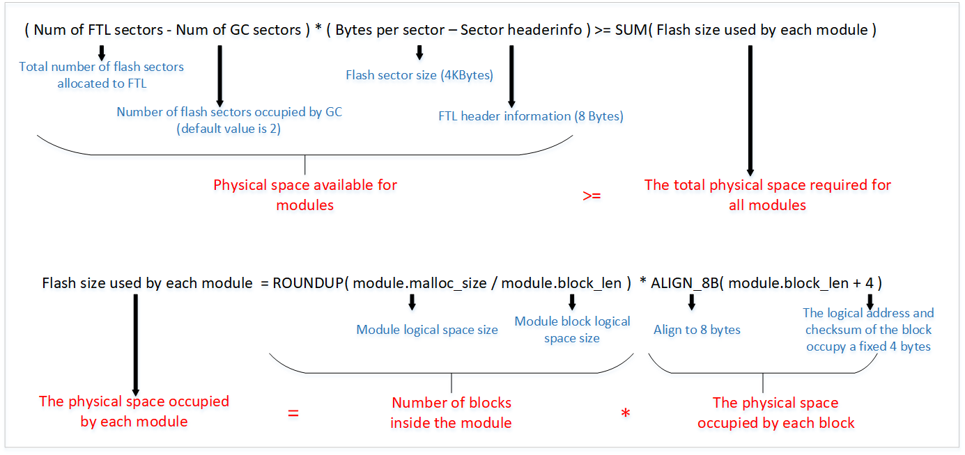
FTLv2 Physical Space Calculation
Additionally, to enhance FTL read efficiency, a mapping table is created for each module to facilitate the conversion between logical and physical addresses. The mapping table for the FTL module occupies RAM space: (malloc_size / block_len * 2Bytes).
备注
Since FTL requires reserved space for the "system module" and GC mechanism, and the FTL physical space is aligned with 4KB, if a smaller flash is chosen and the FTL space needs to be compressed, it must be ensured that the FTL physical space is no less than 16KB. (The FTL reserved space can be adjusted via the otp_config.h parameter, currently unsupported by the SDK).
Flash API
If the FTL size does not meet the requirements, please refer to the flash interfaces described in the section below. There are three basic operations for flash Read, Write and Erase operations. Users should invoke the interfaces described in this section to perform these operations.
Read
Function Name |
flash_nor_read_locked |
|---|---|
Function Prototype |
FLASH_NOR_RET_TYPE flash_nor_read_locked(uint32_t addr, uint8_t *data, uint32_t len) |
Function Description |
read flash data |
Input Parameter |
addr: Read address of flash data: Storage buffer for reading data. Note that the storage buffer cannot be located on flash len: Read data length |
Return Value |
If the reading is successful the returned value is 24 in decimal notation (Corresponding to FLASH_NOR_RET_SUCCESS) |
Prerequisite |
None |
Write
Function Name |
flash_nor_write_locked |
|---|---|
Function Prototype |
FLASH_NOR_RET_TYPE flash_nor_write_locked(uint32_t addr, uint8_t *data, uint32_t len) |
Function Description |
write data to flash |
Input Parameter |
addr: Write address of flash data: Storage buffer for writing data, note that the storage buffer cannot be located on flash len: Write data length |
Return Value |
If the writing is successful the returned value is 24 in decimal notation (Corresponding to FLASH_NOR_RET_SUCCESS) |
Prerequisite |
None |
Erase
Function Name |
flash_nor_erase_locked |
|---|---|
Function Prototype |
FLASH_NOR_RET_TYPE flash_nor_erase_locked(uint32_t addr, FLASH_NOR_ERASE_MODE mode) |
Function Description |
erase flash |
Input Parameter |
addr: erase address of flash FLASH_NOR_ERASE_MODE: erase type of flash |
Return Value |
If the erasing is successful the returned value is 24 in decimal notation (Corresponding to FLASH_NOR_RET_SUCCESS) |
Prerequisite |
None |
flash_nor_erase_locked() supports 3 erase types (FLASH_NOR_ERASE_MODE)
FLASH_NOR_ERASE_SECTOR (4K-Byte)
FLASH_NOR_ERASE_BLOCK(64K-Byte)
FLASH_NOR_ERASE_CHIP
备注
It should be noted that there is no usage scenario of chip erase in a normal application, so chip erase is rarely used.
Bit Modes
Except to the standard Serial Peripheral Interface (SPI), most flash models also support high performance Dual/Quad modes I/O SPI controlled by six pins.
Serial Clock (CLK)
Chip Select (CS#)
Serial Data I/O0 (DI)
Serial Data I/O1 (DO)
Serial Data I/O2 (WP#)
Serial Data I/O3 (HOLD#)
Three Bit Modes
- Single Mode
Standard SPI mode, also called 1 bit-mode, only uses CLK, CS#, DI, and DO pins. WP# is still available for write protect input, and HOLD# is also available for hold input.
- Dual Mode
In 2-bit mode, apart from using CLK and CS#, DI and DO pins become bidirectional I/O pins: I/O0 and I/O1. In comparison to single mode, the functionalities of WP# and HOLD# remain unchanged.
- Quad mode
In 4-bit mode, in addition to using CLK and CS#, DI, DO, WP# and HOLD# are respectively used as I/O0, I/O1, I/O2 and I/O3. As all pins are used in this mode, write protect and hold functions are not available.
备注
RTL87x2G supports two quad mode: STR and DTR. If users need to use the corresponding quad read mode, it is necessary to check flash datasheet or AVL for flash features.
Bit Mode Switch
In order to support as many flash models as possible, single mode (1 bit-mode) is used at ic chip boot time.
If users need to switch to high-speed bit mode (2 or 4 bit mode), please call interface flash_nor_try_high_speed_mode() provided in the SDK.
The parameter "mode" is used to configure bit mode.
If dual mode (2-bit mode) or quad mode (4-bit mode) is selected, the flash is configured and calibrated.
If calibration passed, the bit mode is switched to the selected one.
Otherwise, it is automatically switched back to single mode (1-bit mode).
The prototype of the interface function provided by SDK for bit mode switching is as follows.
Function Name |
flash_nor_try_high_speed_mode |
|---|---|
Function Prototype |
FLASH_NOR_RET_TYPE flash_nor_try_high_speed_mode( FLASH_NOR_IDX_TYPE idx, FLASH_NOR_BIT_MODE mode ) |
Function Description |
switch flash to high-speed bit mode |
Input Parameter |
idx: the default value is FLASH_NOR_IDX_SPIC0 mode: the bit-mode you want to switch to (FLASH_NOR_1_BIT_MODE, FLASH_NOR_2_BIT_MODE, FLASH_NOR_4_BIT_MODE, FLASH_NOR_DTR_4_BIT_MODE) |
Return Value |
If the switching is successful the returned value is 24 in decimal notation (Corresponding to FLASH_NOR_RET_SUCCESS) |
Prerequisite |
None |
Software Block Protect
Although flash supports HW protect pin (#WP) to lock all flash to prevent writing and erasing operations, there are still two disadvantages.
If #WP is used for flash protection, Quad mode (4-bit mode) is not allowed.
Hardware protection can just choose to protect all or protect none, and can’t protect partially.
A mechanism to solve these problems is flash software Blocks Protection (BP). It uses some BP bits in flash status register to select the level (range) to protect as shown in Figure Flash Block Protect.
Flash uses BP(x) bits in status registers to identify number of blocks to lock, and TB bit to determine the locking direction. RTL87x2G only supports locking starting from the low address end of flash.
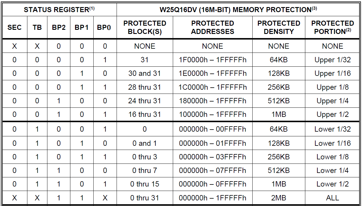
Flash Block Protect
Here we just use BP to protect some important data such as configuration, security, and code sections. Not all portions will be protected.
备注
It should be noted that flash status register by default uses NVRAM type to store data. BP function needs to change (write) BP bits to switch to different protect level, but NVRAM has 100K times programming limitation; although most vendors support 0x50 command to switch using SRAM type, but not all of them support it, such as MXIC.
Not all flash used by RTL87x2G supports proportional block protect (0~1/2~1/4…). GD25WD80C, for instance as Flash Block Protect for GD25WD80C, has a minimum block protect portion of 768KB, which is larger than half. Flash like this could only be locked or unlocked entirely in driver.
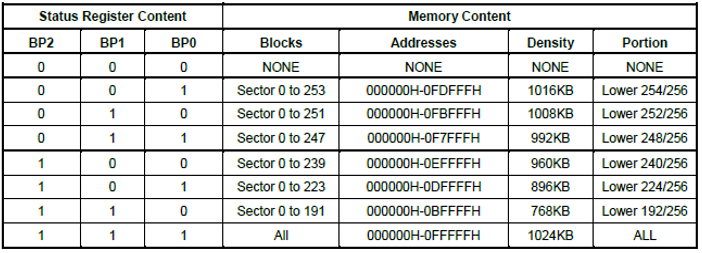
Flash Block Protect for GD25WD80C
APIs are as follows.
Function Name |
flash_nor_set_bp_lv_locked |
|---|---|
Function Prototype |
FLASH_NOR_RET_TYPE flash_nor_set_bp_lv_locked ( FLASH_NOR_IDX_TYPE idx, uint8_t bp_lv ) |
Function Description |
Set flash bp level |
Input Parameter |
idx: the default value is FLASH_NOR_IDX_SPIC0 bp_lv: the bp level you want to set |
Return Value |
If the setting is successful the returned value is 24 in decimal notation (Corresponding to FLASH_NOR_RET_SUCCESS) |
Prerequisite |
None |
Function Name |
flash_nor_get_bp_lv_locked |
|---|---|
Function Prototype |
FLASH_NOR_RET_TYPE flash_nor_get_bp_lv_locked(FLASH_NOR_IDX_TYPE idx, uint8_t *bp_lv) |
Function Description |
get flash bp level |
Input Parameter |
idx: the default value is FLASH_NOR_IDX_SPIC0 bp_lv: storage buffer for getting bp level |
Return Value |
If the getting is successful the returned value is 24 in decimal notation (Corresponding to FLASH_NOR_RET_SUCCESS) |
Prerequisite |
None |
Power Saving
The power mode of flash is mainly divided into three scenarios.
Working: the power consumption is generally around 10 mA.
Standby: the power consumption is typically around the order of 10uA.
Power Down: the power consumption is lower, where it is even less than 1 uA.
Flash automatically enters standby mode without any access, and automatically enters working state when it needs to be accessed again. In order to enter Power Down mode, you need to use a specific command. Most flash use the command 0xB9 to enter into Power Down mode, and use the command 0xAB to exit the Power Down mode. But MXIC toggles the #CS pin to wake up flash.
After flash enters low power mode, it is dangerous to receive commands except for the exit DP command (0xAB). Because flash only accepts wakeup command to exit lower power mode, other commands will be ignored, while flash controller may step into an infinite loop waiting for response from flash.
In order to avoid the risk of calling flash Power Down mode too frequently, the DLPS mechanism in RTL87x2G is equipped with flash Power Down mode control. When entering DLPS, the control flow automatically makes flash enter Power Down mode and wakes up when out of the DLPS.
XIP
XIP (eXecute In Place) is a technique that allows code to be executed directly in flash memory without having to copy it into RAM. This saves RAM space and improves the efficiency of code execution. If the remaining RAM space is sufficient, APP code can be directly executed on RAM, which is conducive to improving performance and reducing power consumption. However, if the APP code is so large that the remaining RAM space is not enough, some or all of the APP codes need to be executed on flash (XIP). Configuration of XIP on RTL87x2G is as follows.
- Macro FEATURE_RAM_CODE (configuration in mem_config.h)a. when configured to 1, any code that does not contain any section modification will be executed on RAM.b. when configured to 0, any code that does not include any section modifiers by default will be executed on flash.
- Section modification (reference app_section.h)a. APP_FLASH_TEXT_SECTION: The specified code is executed on flash.b. APP_RAM_TEXT_SECTION: The specified code is executed on RAM.
备注
If RAM space is insufficient, you should give higher priority to implementing time sensitive code on RAM to ensure efficiency.
- The way to improve the efficiency of XIP execution codeFlash is switched to 2-bit mode or 4-bit mode by calling
flash_nor_try_high_speed_mode().
RTL87x2G can access flash with auto read (directly accessing flash addresses) through SPIC, and execute code directly on SPI flash. However, the operation of accessing flash in user mode is not atomic. Once the accessing is interrupted by higher priority tasks or interrupts, it is possible to cause flash access error. To ensure atomicity of flash operations in user mode, XIP should follow the following restrictions and precautions.
备注
Accessing flash operations in user mode require calling APIs with the "_locked" suffix to ensure a critical area protection. If the time of the flash operation is too long, such as writing a large number of data at one time, it is not suitable for the critical zone protection, and can be split into a small amount of data written by a few times.
If the time-critical interrupt needs to be processed, it is also necessary to ensure that the ISR (interrupt service routine) itself cannot be XIP, and the ISR also prohibits accessing to the flash.