DMA Single Block
This sample demonstrates how to use SPI to transfer data via DMA. Communicate with the flash by SPI via DMA, and then send the data to the PC by UART.
Requirements
The sample supports the following development kits:
Hardware Platforms |
Board Name |
|---|---|
RTL87x2G HDK |
RTL87x2G EVB |
For more requirements, please refer to Quick Start.
Wiring
EVB is connected to W25Q128 module: connect P4_0(SCK) to CLK, P4_1(MISO) to DO, P4_2(MOSI) to DI, P4_3(CS) to CS#.
EVB is connected to FT232 module: connect P3_0 to RX pin of FT232 module and P3_1 to TX pin of FT232 module.
Hardware Introduction
The W25Q128 is a NOR Flash chip with SPI interface, which support the standard Serial Peripheral Interface (SPI), Dual/Quad I/O SPI as well as 2-clocks instruction cycle Quad Peripheral Interface (QPI).
Additionally, the device supports JEDEC standard manufacturer and device ID and SFDP Register, a 64-bit Unique Serial Number and three 256-bytes Security Registers.
Additional details can be found in the application guide for this device. In this example the device is used as slave for SPI communication test.
Building and Downloading
This sample can be found in the SDK folder:
Project file: samples\peripheral\spi\gdma_singleblock\proj\rtl87x2g\mdk
Project file: samples\peripheral\spi\gdma_singleblock\proj\rtl87x2g\gcc
To build and run the sample, follow the steps listed below:
Open Sample Project File.
To build the target, follow the steps listed on the Generating App Image in Quick Start.
After a successful compilation, the app bin
app_MP_xxx.binwill be generated in the directorymdk\binorgcc\bin.To download app bin into EVB board, follow the steps listed on the MPTool Download in Quick Start.
Press reset button on EVB board and it will start running.
Experimental Verification
After initialization, the DMA starts to carry TX data. When the transmission completes, it enters the GDMA TX interrupt and prints the LOG.
GDMA_TX_Channel_Handler: TX completed!
The SPI receives the data sent back from the external flash and the DMA starts to carry the RX data. When the handling is finished, it enters the GDMA RX interrupt and prints the length of the acquired data and the data information.
GDMA_RX_Channel_Handler!
[io_gdma] io_handle_gdma_msg: read data complete,data_len = 3
GDMA_Recv_Buffer[0] = 0x000000ef
GDMA_Recv_Buffer[1] = 0x00000040
GDMA_Recv_Buffer[2] = 0x00000018
The UART sends the received data via FT232 to the serial assistant on the PC, and receive the JEDEC_ID information on the serial assistant.
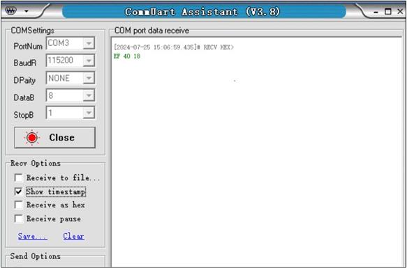
Message received by the Serial Assistant
Code Overview
This chapter will be introduced according to the following several parts:
Peripheral initialization will be introduced in chapter Initialization .
Functional implementation after initialization will be introduced in chapter Functional Implementation .
Source Code Directory
Project Directory:
sdk\samples\peripheral\spi\gdma_singleblock\projSource Code Directory:
sdk\samples\peripheral\spi\gdma_singleblock\src
Source files are currently categorized into several groups as below.
└── Project: gdma_singleblock
    └── secure_only_app
        └── Device                   includes startup code
            ├── startup_rtl.c
            └── system_rtl.c
        ├── CMSIS                    includes CMSIS header files
        ├── CMSE Library             Non-secure callable lib
        ├── Lib                      includes all binary symbol files that user application is built on
            └── rtl87x2g_io.lib
        ├── Peripheral               includes all peripheral drivers and module code used by the application
            ├── rtl_rcc.c
            ├── rtl_pinmux.c
            ├── rtl_nvic.c
            ├── rtl_uart.c
            ├── rtl_gdma.c
            └── rtl_spi.c
        └── APP                      includes the ble_peripheral user application implementation
            ├── main_ns.c
            ├── io_uart.c
            ├── io_gdma.c
            └── io_spi.c
Initialization
The initialization process includes board_spi_init , board_uart_init , driver_uart_init and driver_spi_gdma_init.
board_spi_init contains the PAD and PINMUX settings of SPI.
Config PAD: Set pins as PINMUX mode, PowerOn, internal pull-up.
Config PINMUX: Assign pins for SPI0_CLK_MASTER, SPI0_MO_MASTER, SPI0_MI_MASTER, SPI0_CSN_0_MASTER functions respectively.
board_uart_init contains the PAD and PINMUX settings of UART.
Config PAD: Set pins as PINMUX mode, PowerOn, internal pull-up.
Config PINMUX: Assign pins for UART0_TX, UART0_RX functions respectively.
driver_uart_init contains the initialization of UART peripheral.
Enable PCC clock.
Set no parity.
Set stop bits 1 bit.
Set word lenth 8 bit.
RCC_PeriphClockCmd(APBPeriph_UART0, APBPeriph_UART0_CLOCK, ENABLE);
...
UART_InitStruct.UART_Parity         = UART_PARITY_NO_PARTY;
UART_InitStruct.UART_StopBits       = UART_STOP_BITS_1;
UART_InitStruct.UART_WordLen        = UART_WORD_LENGTH_8BIT;
UART_InitStruct.UART_RxThdLevel     = 16;
UART_InitStruct.UART_IdleTime       = UART_RX_IDLE_2BYTE;
driver_spi_gdma_init contains the initialization of SPI and GDMA peripheral.
Initialize the SPI peripheral:
Enable PCC clock.
Set the communication mode to EEPROM mode.
Refer to SPI Polling initialization flow for other basic settings.
Set NDF to GDMA_READ_SIZE_MAX.
Enable GDMA TX and RX for SPI.
Set the TxWaterlevel to SPI_TX_FIFO_SIZE - 8, set the RxWaterlevel to 8 - 1.
RCC_PeriphClockCmd(APBPERIPH_SPI, APBPERIPH_SPI_CLOCK, ENABLE);
...
SPI_InitStructure.SPI_Direction   = SPI_Direction_EEPROM;
...
SPI_InitStructure.SPI_NDF         = GDMA_READ_SIZE_MAX;
SPI_InitStructure.SPI_RxDmaEn     = ENABLE;
SPI_InitStructure.SPI_TxDmaEn     = ENABLE;
SPI_InitStructure.SPI_RxWaterlevel = 8 - 1;
SPI_InitStructure.SPI_TxWaterlevel = SPI_TX_FIFO_SIZE - 8;
Initialize the GDMA TX:
Enable PCC clock.
Use GDMA channel 3.
Transfer direction is memory to peripheral transfer.
Set the source address to increment and the destination address to be fixed.
Set the source and destination MSize to GDMA_Msize_8.
The source address is
GDMA_WriteCmdBuffer, and the destination address isFLASH_SPI->SPI_DR.Configure the GDMA TX total transfer completion interrupt
GDMA_INT_Transfer.
RCC_PeriphClockCmd(APBPeriph_GDMA, APBPeriph_GDMA_CLOCK, ENABLE);
...
GDMA_InitStruct.GDMA_ChannelNum          = GDMA_TX_CHANNEL_NUM;
GDMA_InitStruct.GDMA_DIR                 = GDMA_DIR_MemoryToPeripheral;
GDMA_InitStruct.GDMA_SourceInc           = DMA_SourceInc_Inc;
GDMA_InitStruct.GDMA_DestinationInc      = DMA_DestinationInc_Fix;
GDMA_InitStruct.GDMA_SourceMsize         = GDMA_Msize_8;
GDMA_InitStruct.GDMA_DestinationMsize    = GDMA_Msize_8;
...
GDMA_InitStruct.GDMA_SourceAddr          = (uint32_t)GDMA_WriteCmdBuffer;
GDMA_InitStruct.GDMA_DestinationAddr     = (uint32_t)FLASH_SPI->SPI_DR;
...
GDMA_INTConfig(GDMA_TX_CHANNEL_NUM, GDMA_INT_Transfer, ENABLE);
...
Initialize GDMA RX:
Enable PCC clock.
Use GDMA channel 0.
Transfer direction is peripheral to memory transfer.
Set the source address to be fixed and the destination address to be incremented.
Set the source and destination MSize to GDMA_Msize_8.
The source address is
FLASH_SPI->SPI_DRand the destination address isGDMA_Recv_Buffer.Configure the GDMA RX total transfer completion interrupt
GDMA_INT_Transfer.
RCC_PeriphClockCmd(APBPeriph_GDMA, APBPeriph_GDMA_CLOCK, ENABLE);
...
GDMA_InitStruct.GDMA_ChannelNum          = GDMA_RX_CHANNEL_NUM;
GDMA_InitStruct.GDMA_DIR                 = GDMA_DIR_PeripheralToMemory;
GDMA_InitStruct.GDMA_SourceInc           = DMA_SourceInc_Fix;
GDMA_InitStruct.GDMA_DestinationInc      = DMA_DestinationInc_Inc;
GDMA_InitStruct.GDMA_SourceMsize         = GDMA_Msize_8;
GDMA_InitStruct.GDMA_DestinationMsize    = GDMA_Msize_8;
...
GDMA_InitStruct.GDMA_SourceAddr          = (uint32_t)FLASH_SPI->SPI_DR;
GDMA_InitStruct.GDMA_DestinationAddr     = (uint32_t)GDMA_Recv_Buffer;
...
GDMA_INTConfig(GDMA_RX_CHANNEL_NUM, GDMA_INT_Transfer, ENABLE);
Set the data receive length in EEPORM transmission mode to 3 (JEDEC_ID length is 3), enable SPI.
Set the Buffer Size for GDMA TX and RX, enable RX GDMA and enable TX GDMA.
SPI_SetReadLen(SPI0, 3);
SPI_Cmd(FLASH_SPI, ENABLE);
GDMA_SetBufferSize(GDMA_RX_Channel, 3);
GDMA_Cmd(GDMA_RX_CHANNEL_NUM, ENABLE);

/* Send read data command */
GDMA_SetBufferSize(GDMA_TX_Channel, 1);
GDMA_SetSourceAddress(GDMA_TX_Channel, (uint32_t)GDMA_WriteCmdBuffer);
GDMA_Cmd(GDMA_TX_CHANNEL_NUM, ENABLE);
Functional Implementation
After enabling the GDMA TX channel, trigger the GDMA TX transfer, trigger the
GDMA_INT_Transferinterrupt after the transfer is completed, and execute the interrupt handler functionGDMA_RX_Channel_Handler.Disable the GDMA TX channel interrupt, print the entry interrupt message, clear the GDMA interrupt pending bit, and enable
GDMA_INT_Transferinterrupt.
After receiving the message of GDMA TX transfer, flash transfers the internal information back through the GDMA RX channel. Once the transfer is complete, it triggers the
GDMA_INT_Transferinterrupt, and enters the interrupt handler functionGDMA_RX_Channel_Handler.Disable the GDMA TX channel interrupt, print the GDMA_Recv_Buffer information.
Execute
uart_senddata_continuousto send the GDMA_Recv_Buffer information to the PC via UART0.
GDMA_INTConfig(GDMA_RX_CHANNEL_NUM, GDMA_INT_Transfer, DISABLE);

uint16_t data_len = (GDMA_TRANSFER_SIZE);
for (uint16_t i = 0; i < GDMA_TRANSFER_SIZE; i++)
{
    DBG_DIRECT("GDMA_Recv_Buffer[%d] = 0x%x", i, GDMA_Recv_Buffer[i]);
}
uart_senddata_continuous(UART0, GDMA_Recv_Buffer, data_len);

GDMA_ClearINTPendingBit(GDMA_RX_CHANNEL_NUM, GDMA_INT_Transfer);
GDMA_INTConfig(GDMA_RX_CHANNEL_NUM, GDMA_INT_Transfer, ENABLE);
Troubleshooting
When the SPI frequency to be used is high (greater than 10MHz), it is recommended to use DMA to transfer data. If it is found that the CS line is pulled up during data transfer, the MSize of GDMA can be increased to improve the transfer efficiency of DMA.