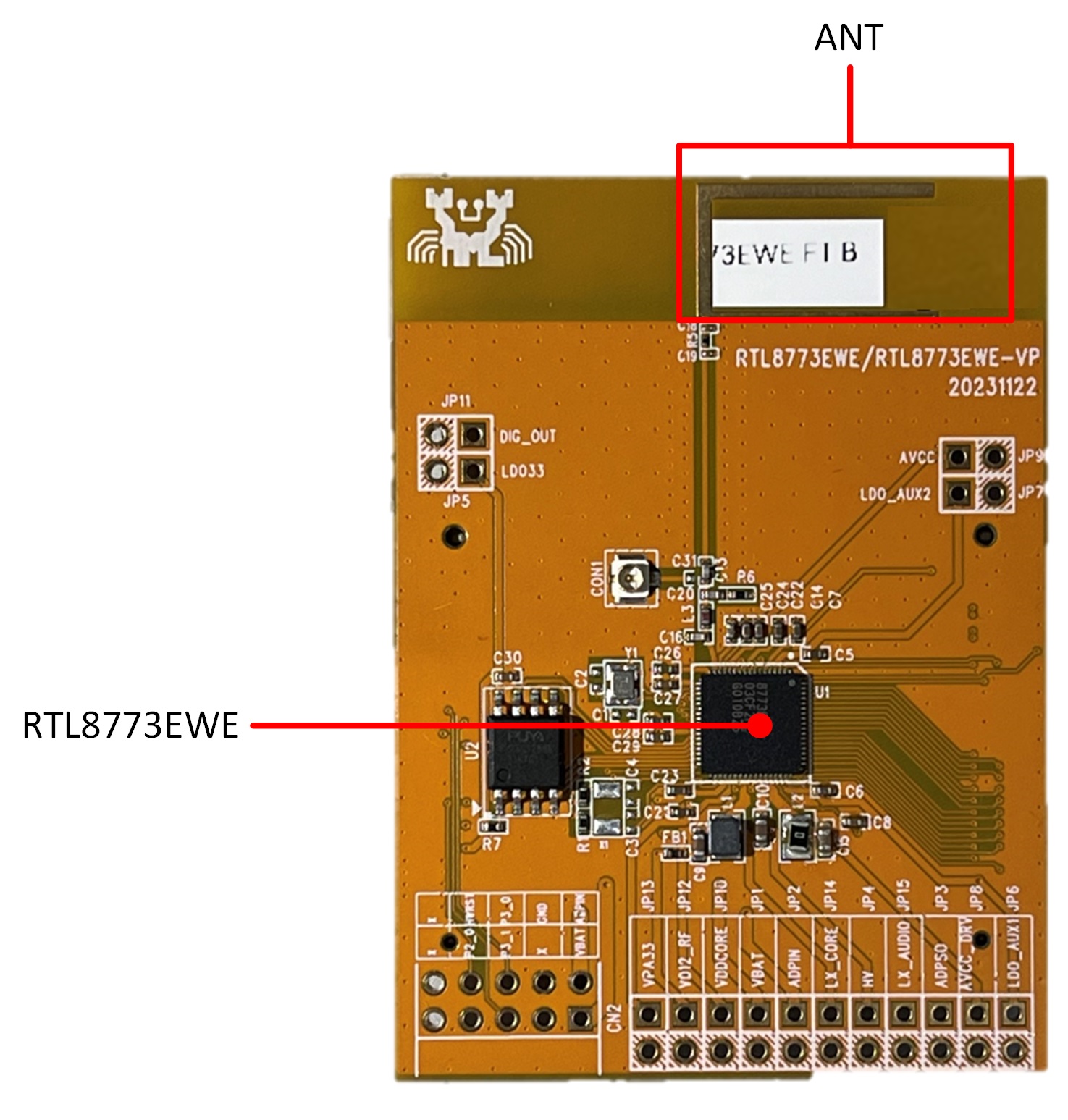
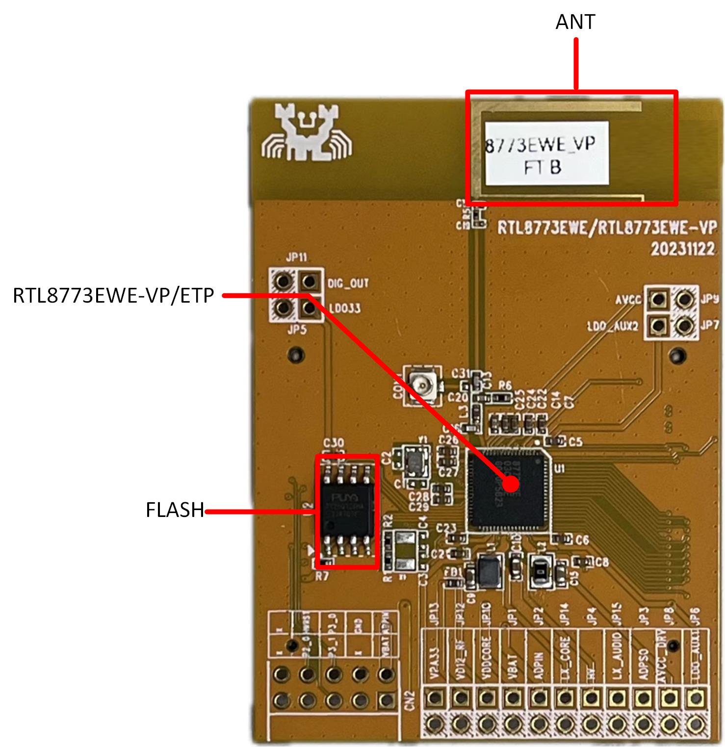
RTL8773E evaluation board is compatible with the following daughter boards, RTL8773EWE-VP and RTL8773ETP share the same EVB; the only difference is the chip:
VADP power supply RTL8773EWE daughter board ADPIN, can be powered by CON1 USB5V or CON2 UFN5V.
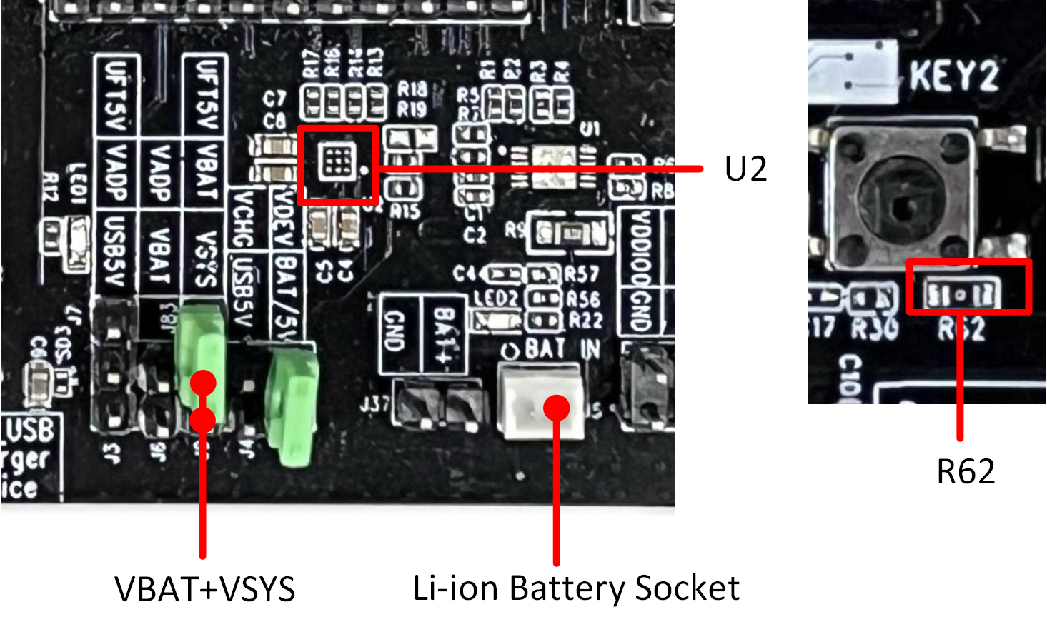
MP2661 Charger Chip
Allowed to control charging current with I2C interface, powered by 5V from CON1 USB socket, supply power for RTL8773E daughter board from VSYS pin, not mounted by default, need to solder U2 and remove R62 when applying the external charger.
LCD display screen with TP connector, dedicated LCDCQSPI/ I8080 pins assigned. It could work with RTK 1.96-inch QSPI/LCD screen module.
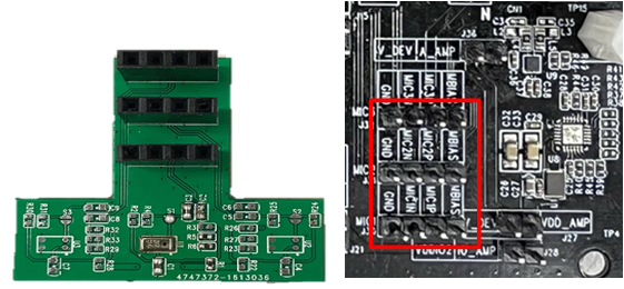
Hardware Echo Cancellation Sampling Circuit
The signal output by the external analog amplifier is connected to the MIC2 input through the hardware echo cancellation sampling circuit as the reference signal for echo cancellation, so as to prevent the external analog amplifier from entering the nonlinear region and causing the echo cancellation to be unclean. Not mounted by default, need to solder.
The three independent buttons KEY1, KEY2, and KEY3 are respectively connected to P3_0, ADC_0, and P3_1.
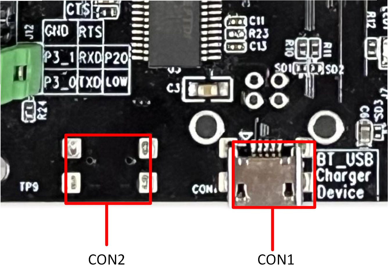
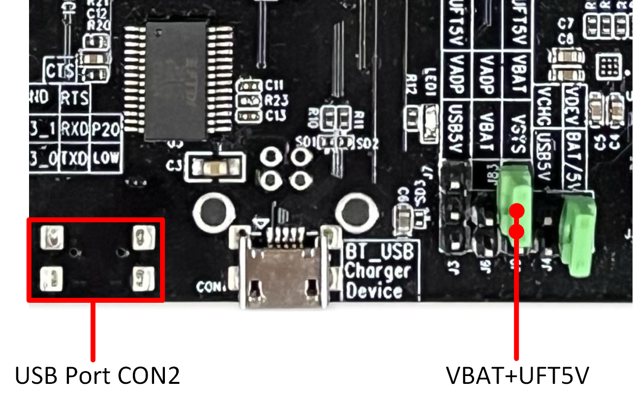
USB Port CON2
Connect to FT232, USB to serial UART converter chip. This interface is mainly used for UART downloading or log debugging. It is also allowed to choose this USB to supply power for VBAT with jumper.
Evaluation Board Pin Assignment and IO Using Notes
There is an anti-reverse insertion mechanism between mother board and daughter board. Please refer to the following table about the specific pin assignment of daughter board
RTL8773E_IOPin_Information.
Note
P3_4, P3_5 are connected with 32K crystal by default. Solder R1, R2 on RTL8763EW daughter board, or R5, R6 on RTL8763EW daughter board if using GPIO function instead.
The feature of internal PSRAM is as follows: RTL8773EWE-VP supports internal PSRAM, while RTL8773EW does not support internal PSRAM.
P1_0, P1_1 are assigned to be quadrature encoder input, with 0.1uF capacitor for debouncing. If P1_0, P1_1 are used for high-speed interface, please remove C23, C24 near J16 connector.
Here is an introduction to the power on, download, and normal mode connection of RTL8773E evaluation board on hardware.
Evaluation Board Power Connection
RTL8773E evaluation board power supply can be powered separately using USB port CON2, but it can download programs normally. Please refer to IC Power Source Selection for details, VBAT connection for internal charger without lithium battery.
RTL8773E evaluation board does not support USB communication function.
Download Mode Connection
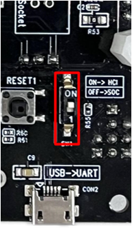
P2_0 pin is the selection pin of downloading mode. Pull P2_0 low, and then repower IC or hardware reset, so that SoC will bypass flash code and enter downloading mode. FT_VIO (FT232 VDDIO) connects to VDDIO0 (HCI UART IO domain), and ensure P3_1->RXD, P3_0->TXD, then set the dial switches SW1 ON position(which will pull down the LOG pin)and then power on the board or perform a hardware reset to enter download mode.
After the program download is complete, set the dial switches SW1 back to the 1 position, allowing P2_0 to return to a floating state. Finally, press the hardware reset button or power cycle the board, and the program will run normally.
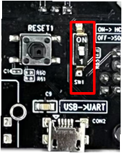
Please confirm that the dial switches SW1 are set to the 1 position, then place the jumper on the red box in the figure below. Connect P2_0 (log) to RXD. FT_VIO (FT232 VDDIO) connects to VDDIO1. P3_0 and P3_1 are disconnected from RX and TX respectively. On the computer side, use the Debug Analyzer software tool via the USB port CON2 to read the operating information of the sub-board chip.
Here is an introduction to the usage and tips of blocks and interfaces on RTL8773E evaluation board.
EVB Daughter Board
EVB daughter board can be removed and replaced. There is an anti-reverse insertion mechanism between mother board and daughter board.
RTL8773EWE and RTL8773EWE-VP daughter boards are compatible with the RTL8773E evaluation board.
USB Port CON1 is used for evaluating board power supply, connecting USB to RTL8773E, for RTL8773E USB communication and external charger charging. Due to VDD_DEV power supply requirements, the D2 diode has been removed, otherwise VBAT will backflow into USB 5V, and currently this port cannot be used for power supply.
USB Port CON2
USB Port CON2 is used for evaluating board power supply, connecting USB to UART chip FT232, this interface is mainly used for UART download or debugging log connection. Jumpers can be used to power VBAT from this USB.
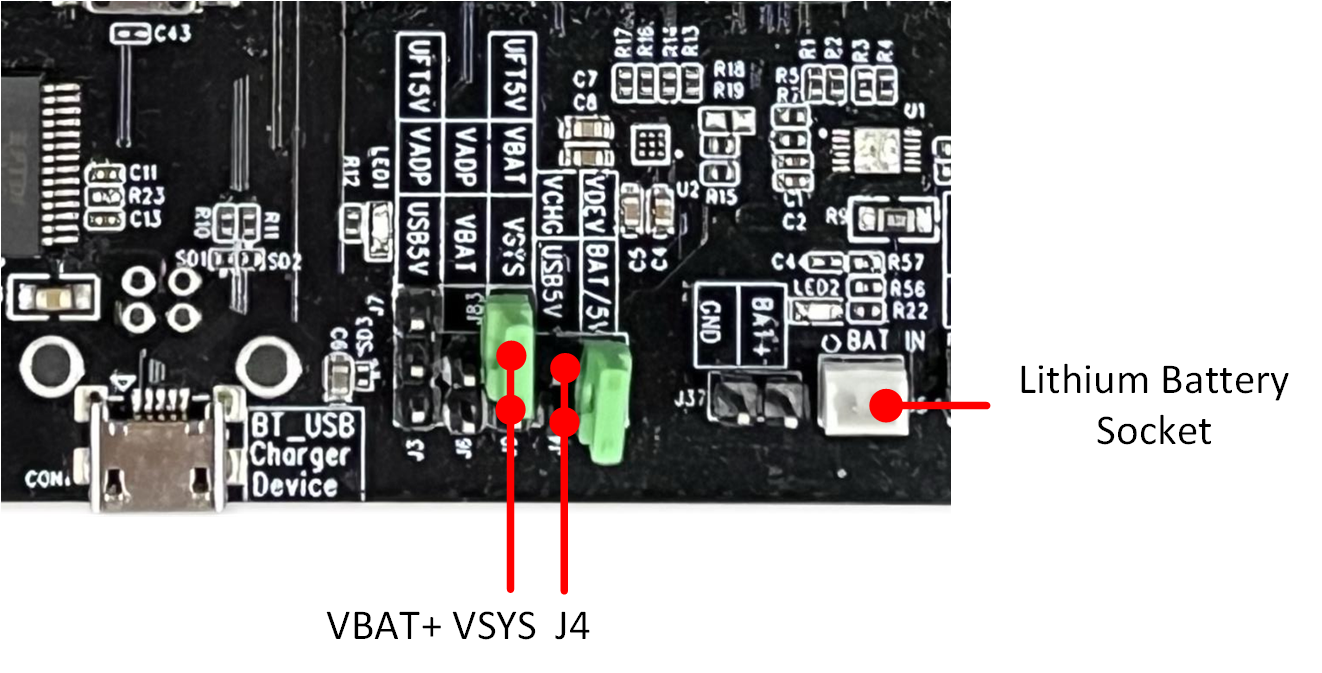
RTL8773E evaluation board supports lithium battery socket, under the power supply of a lithium battery. If using the U2 external charging chip MP2661, the lithium battery can be connected to J5 or J37 and short circuited to J9’s VBAT and VSYS. Remove R62 below KEY2 and use the charging chip VSYS to power VBAT; if the external charging chip is not installed, it is necessary to confirm that R62 is installed, and then short-circuit the VBAT and VSYS of J9.
RTL8773E Evaluation Board Powered by Lithium Battery
IC Power Source Selection
Internal Charger Power Supply
VBAT has two types of power supply, lithium battery power supply or USB power supply. It can connect VBAT and UFT5V of J9, powered by FT_5V of the reverse USB socket CON2 to VBAT; choose one of the two connection methods, do not connect them at the same time, otherwise it may be dangerous to directly connect the USB 5V to the battery.
The EVB is equipped with MP2661 to meet the external charging requirement. The charging current of MP2661 is 535mA maximum under CC state, 246mA by default, 20mA under precharge state. When used, lithium battery should be inserted into J5(Molex ZH1.25), while USB should be connected to the USB socket CON1. Short J4 VCHG and USB5V, J9 VBAT and VSYS, and the charging current could be set by I2C.
RTL8773E Evaluation Board External Charger Power Supply
Note
When using internal charger, RTL8773E VBAT recommended operation voltage range is 2.8V~4.35V. If using the internal charger, the method of powering VBAT with FT_5V is only restricted to developing, debugging EVB for easy operation. In the mass production phase, do not power VBAT exceed 4.35V due to the risk of flowing backward ADPIN.
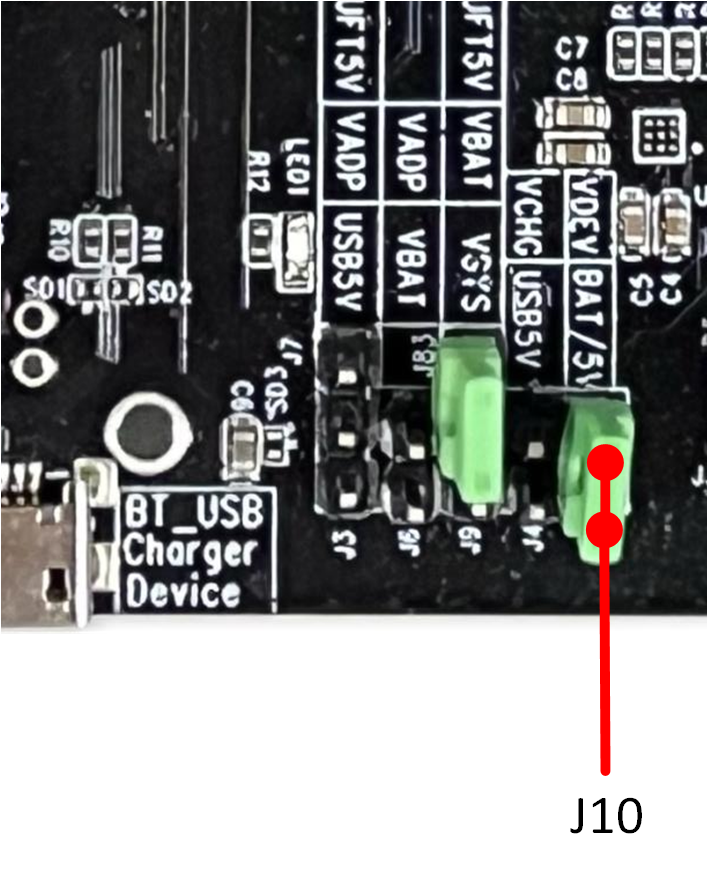
VDD_DEV supply power to Smart PA/Analog PA/SD Nand flash/LCD screen module with shorting J10. Note that the BAT/5V pin header is actually powered by the VBAT/USB_5V through a Schottky diode. As it is found in the actual test that VBAT will flow backward to USB5V resulting in USB insertion error detection. At present, the D2 diode has been removed, and USB 5V (CON1 USB socket) cannot be used to power the Device.
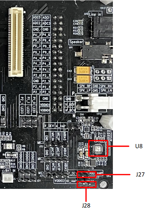
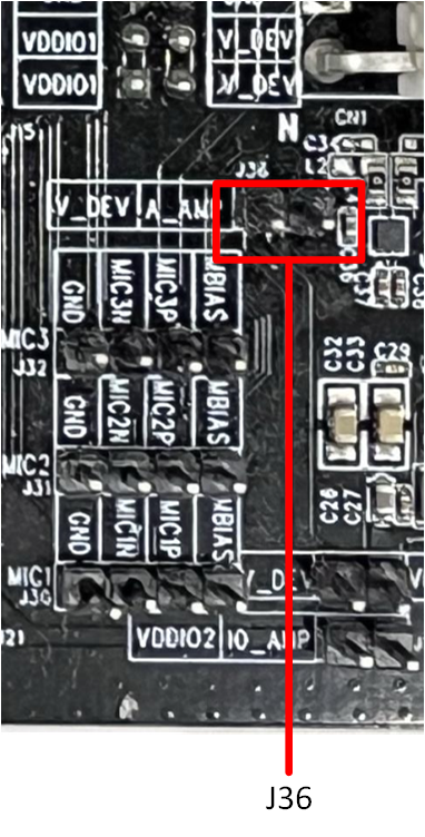
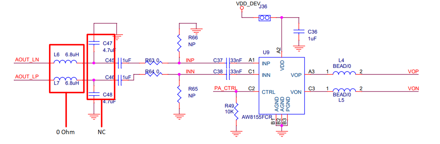
RTL8773E evaluation board support AW8155FCR Analog Audio Amplifier, before using on-board analog PA AW8155FCR, you need to ensure J36 is short. Since the digital and analog amplifiers on EVB share the same output interface, you need to solder L4, L5 before using AW8155FCR. By default, L4/L5 are mounted. PA output applies VH3.96 interface, and it is allowed to buy connect wire online to solder with the speaker.
In addition, due to the shared mother board between RTL8773E and RTL8763E, RTL8763E has a Class D output, and a set of LC filters is added between RTL8763E and the amplifier. But RTL8773E is a Class A/B output and no longer requires LC filtering. It is recommended to replace L6 and L7 with 0 ohm resistors and leave C47 and C48 NC.
RTL8773E Evaluation Board Analog Audio Amplifier Circuit
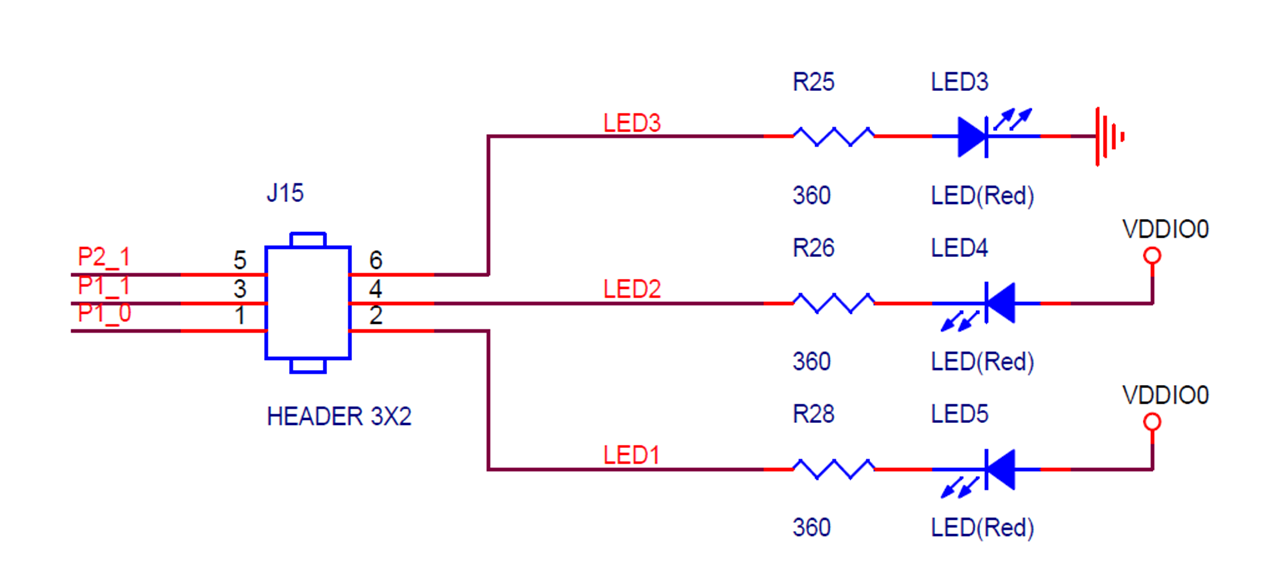
LED Module
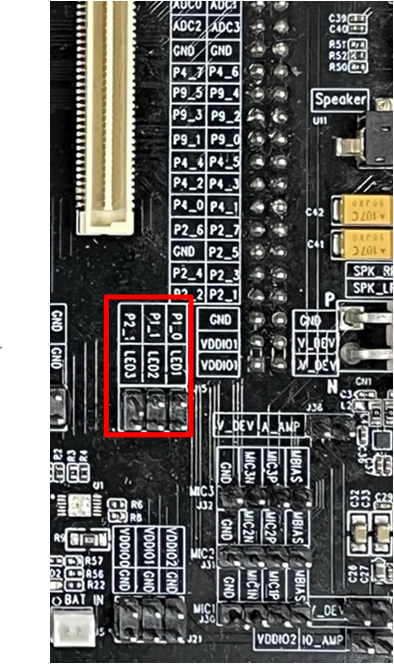
The LED module provides 3 red LEDs and supports sleep LED function, which can be connected to the pin header inside the red frame through a jumper cap. It is worth noting that LED1 and LED2 are active-low, while LED3 is active-high.
RTL8773E Evaluation Board Red LED Module Schematic
Earphone Socket
Earphone jack U11, support 3.5mm plug stereo earphone. The audio output of RTL8773E is Class A/B, with weak driving capability, and only allows loading loads of 10K ohm or more. If directly connected to 16/32 ohm earphones, it will result in a decrease in volume and poorer audio performance. The best solution behind the headphone jack is to connect an audio amplifier with a balanced interface. After the amplifier is amplified, the speaker can be pushed. The amplifier can be an onboard analog amplifier.
The earphone jack can also be plugged into a plug-in Small Speaker. However, the small speakers on the market are single-ended inputs. This connection is equivalent to leaving the RTL8773E differential output negative, resulting in a poor anti-jamming output and the possibility of importing pop sounds.
J35 is used for screen display function, and contains LCDC QSPI/I8080 interface. You can choose RTK LCD screen board, equipped with a 1.96-inch screen with capacitive touch function, to achieve human-machine interaction. For details about the schematic and specifications, refer to the information of the LCD screen.
Need to set the DIP switches SW1 ON position, which will pull down the LOG pin or J12 connected, then press reset button or power on again to enter download mode. Please refer to Download Mode Connection.
Need to set the DIP switches SW1 1 position, which will pull none the LOG pinor J12 disconnected, then press reset button or power on again to start running the program. Log pin can be used for debug. Please refer to Normal Mode Connection .