RTL8773EWP
RTL8773EWP evaluation board is compatible with the following daughter boards:
RTL8773EWP evaluation board provides a hardware environment for user development, including:
Support Wi-Fi module and SD Nand Flash module interface
Lithium battery socket ZH1.25
Support infrared sensing interface
Support temperature and humidity sensor interface
Note
To purchase EVB, please visit https://www.realmcu.com/en/Home/Shop.
EVB Blocks Distribution
Distribution diagrams of blocks on the front and back of the RTL8773EWP evaluation board are as following:
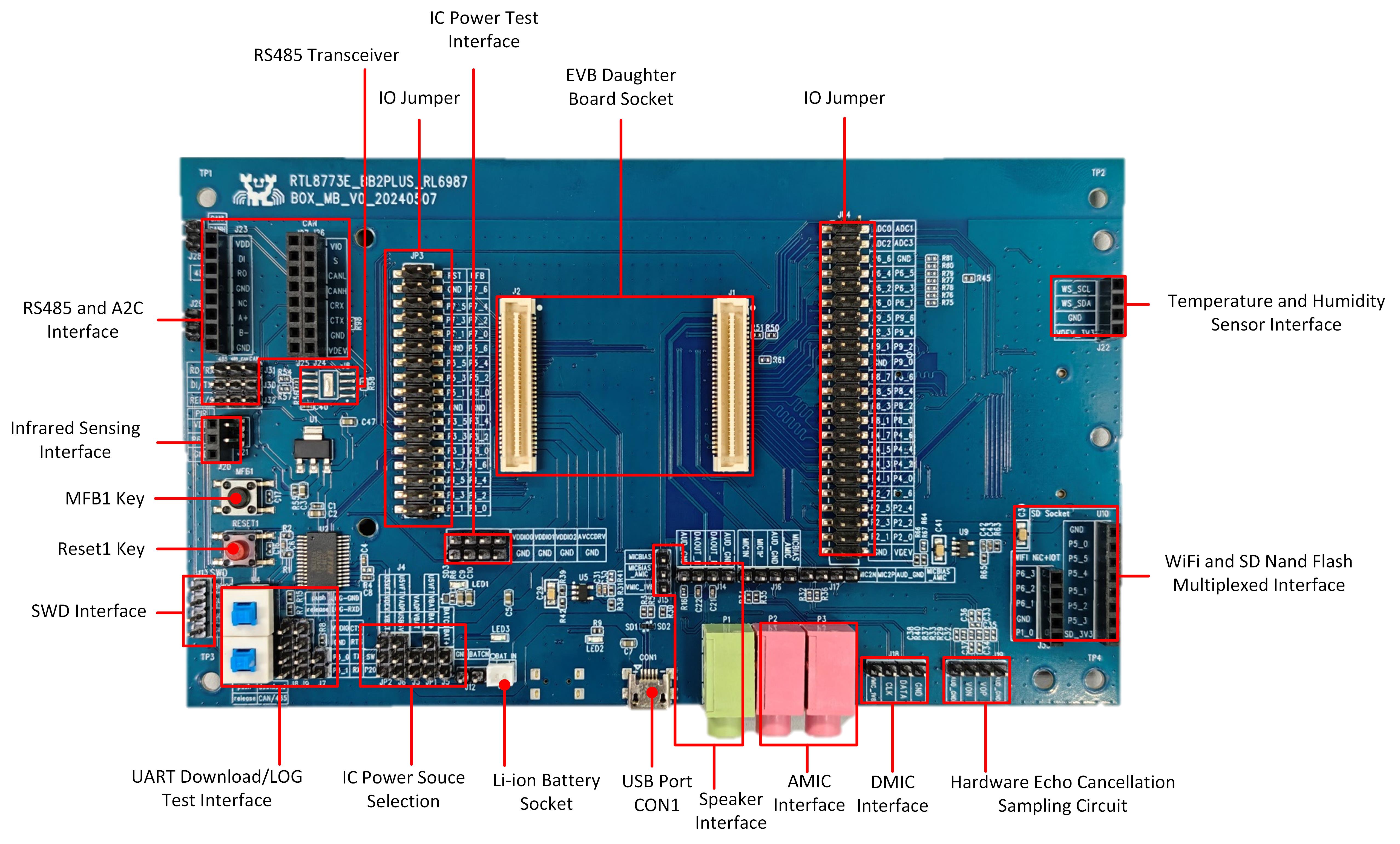
EVB RTL8773EWP Blocks Distribution Diagram-Front
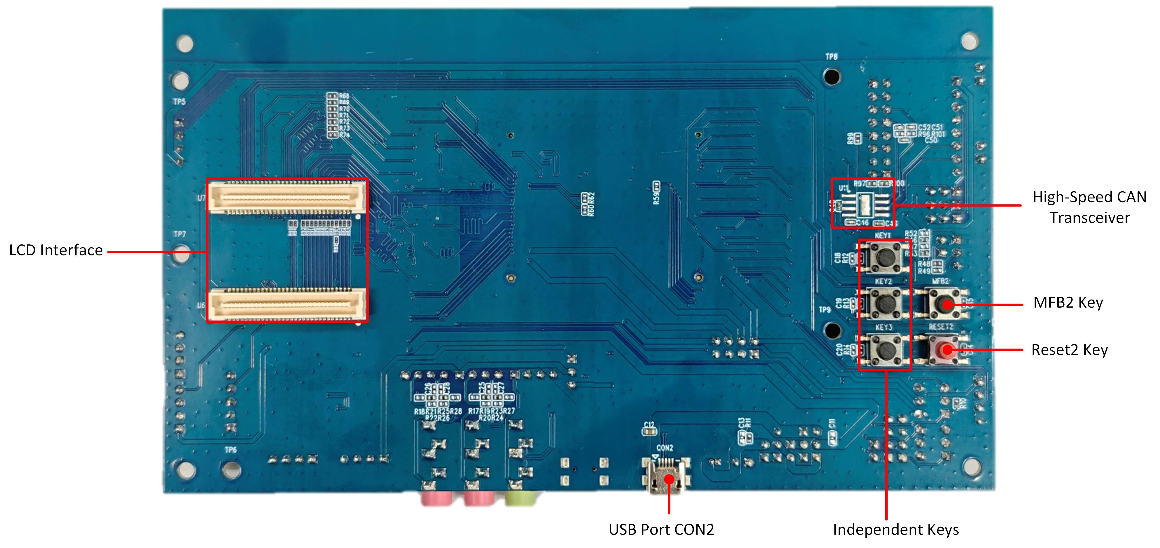
EVB RTL8773EWP Blocks Distribution Diagram-Back
The following introduces the main blocks on the evaluation board in counterclockwise order.
Blocks |
Introduction |
|---|---|
EVB Daughter Board Socket |
Used to connect the EVB daughterboard with an anti-reverse insertion mechanism. |
IC Power Test Interface |
Used to test the IC’s internal power supply. |
IO Jumper |
Used to peripheral device connection and providing I/O test interfaces. |
RS485 Transceiver |
Used to peripheral device connection and providing I/O test interfaces. |
Used to connect the RS485 and the A2C modules. |
|
Used to connect the infrared sensor module. |
|
MFB1 Key |
Multi-functional buttons, which shares MFB connection with MFB2. |
Reset1 Key |
Pressing this key reset the system. |
SWD Interface |
Used to SWD debug. |
Supports download mode and normal mode. |
|
IC Power Source Selection |
IC Power Source Selection (USB-CON2 / Lithium Battery Optional) |
Li-ion Battery Socket |
Used to 2-Pin Interface for Single-Cell Li-ion Battery Connection. |
USB Port CON1 |
Used USB_5V to power EVB for charging or device. |
Supports 3.5mm audio interface. |
|
Supports 3.5mm audio interface and pin headers for the external AMIC daughterboard. |
|
Audio Amplifier Output Hardware Feedback Circuit for echo cancellation. |
|
Hardware Echo Cancellation Sampling Circuit |
Audio Amplifier Output Hardware Feedback Circuit for echo cancellation. |
Used to connect to Wi-Fi module or RTK SD Nand Flash daughterboard. |
|
Used to connect to the temperature and humidity sensor. |
|
Used to connect to the display screen. |
|
USB Port CON2 |
Used to power the EVB and connect USB to UART chip FT232RL for downloading programs or debugging. |
Independent Keys |
Three Independent Buttons (KEY1, KEY2, KEY3) connected to ADC_2, P2_1, and P3_5 respectively. |
Reset2 Key |
Pressing this key reset the system. |
MFB2 Key |
Multi-functional buttons, which shares MFB connection with MFB1. |
High-Speed CAN Transceiver |
CAN Bus Interface (Not populated by default; install U11 TJA1049 when required). |
EVB Interfaces Distribution
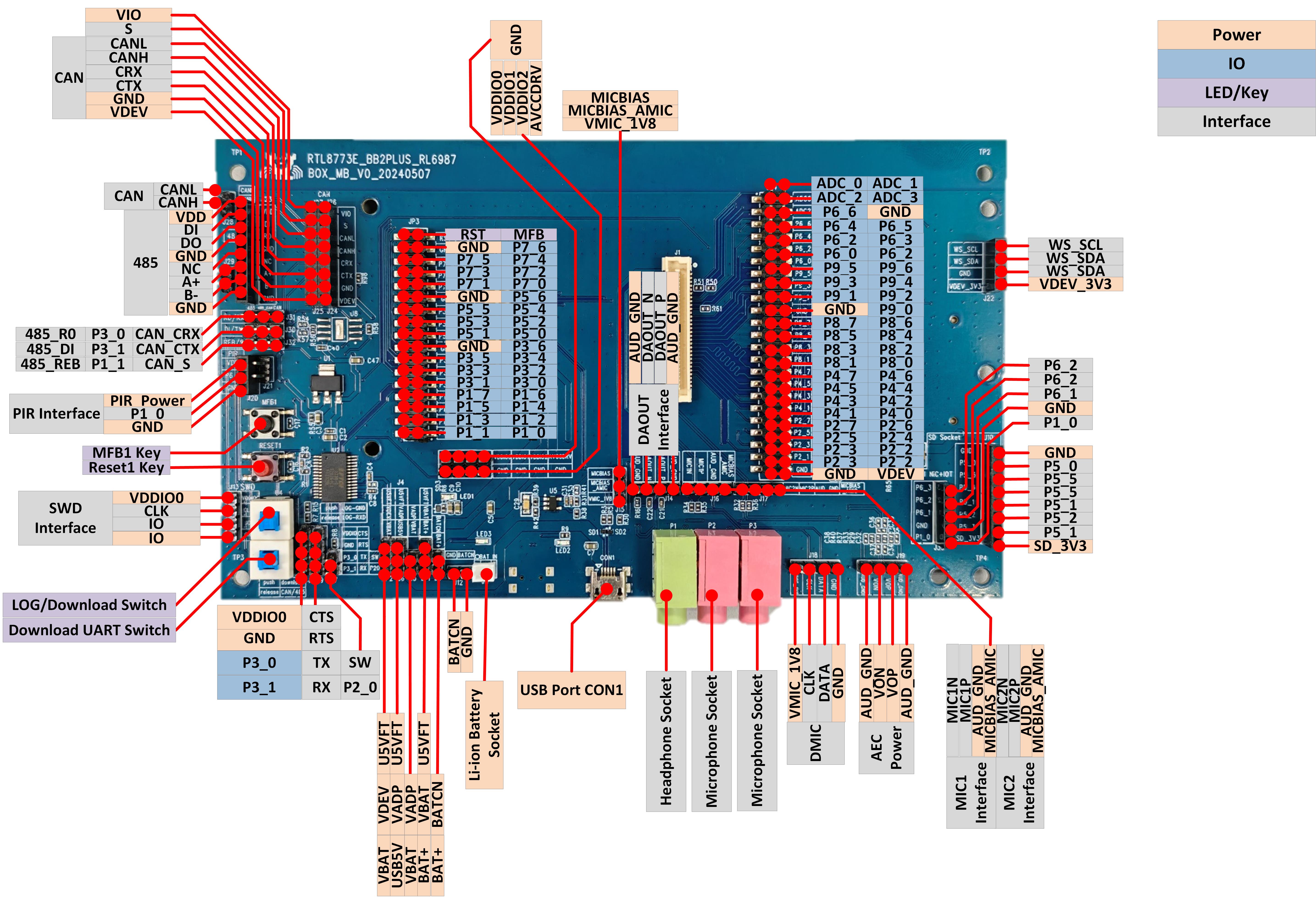
EVB RTL8773EWP Interfaces Distribution Diagram-Front
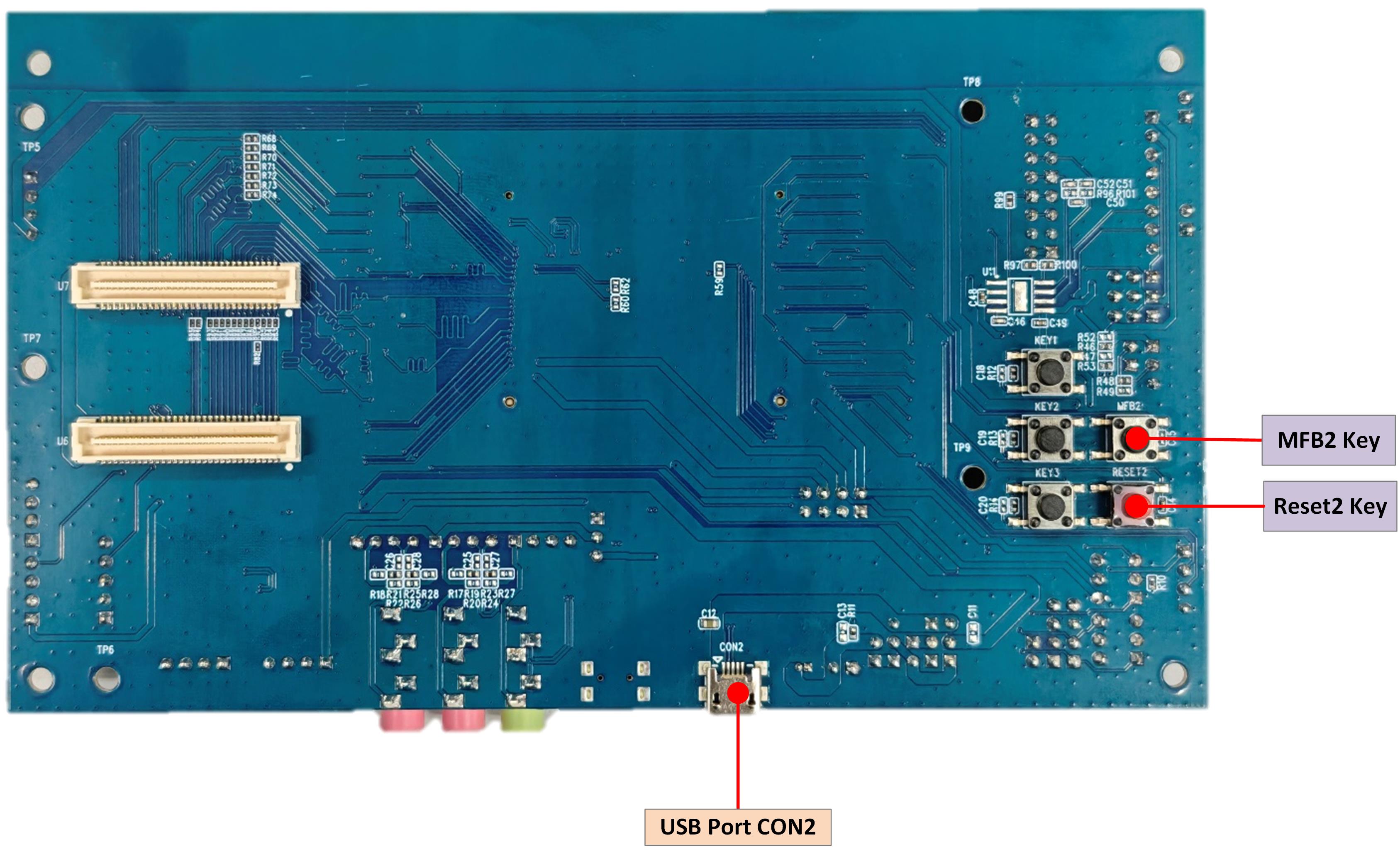
EVB RTL8773EWP Interfaces Distribution Diagram-Back
Evaluation Board Pin Assignment and IO Using Notes
The connectors between the daughter board and the main board have an anti-reverse mechanism. The specific pin assignments of the daughter board can be found in the following table.:
RTL8773EWP_Pinassignment_Information.
Note
RTL8773EWP chip supports internal PSRAM.
Evaluation Board User Guide
Here is an introduction to the power on, download, and normal mode connection of RTL8773EWP evaluation board on hardware.
-
Evaluation Board Power Connection
The RTL8773EWP evaluation board can be powered solely through the USB port CON2, which also supports image downloading and recording logs. The power connection for the evaluation board is shown in the diagram below. The USB port marked with a red box must be connected, and the locations marked with red dots should be bridged with jumpers, as shown in figure.
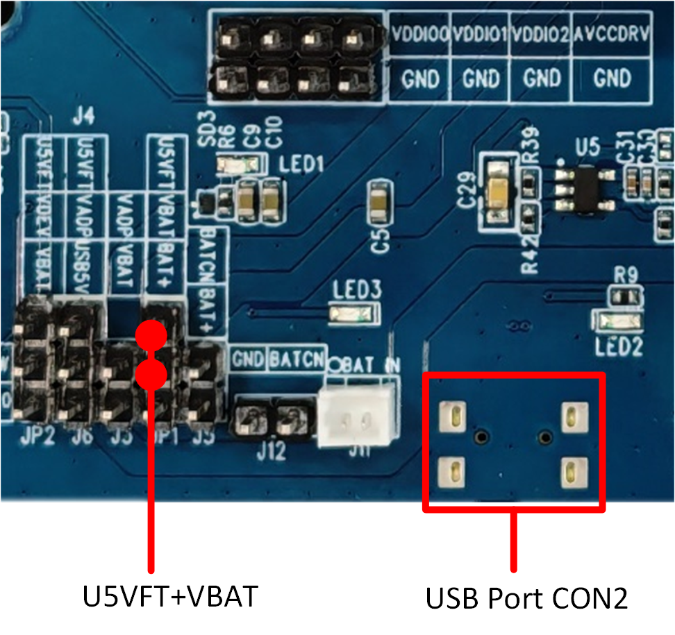
USB CON2 Charger Power Supply
-
Download Mode Connection
P2_0 is the download mode selection pin. When P2_0 is pulled low and the board is powered on again or a hardware reset is performed, the flash code will be bypassed and the system will enter download mode.
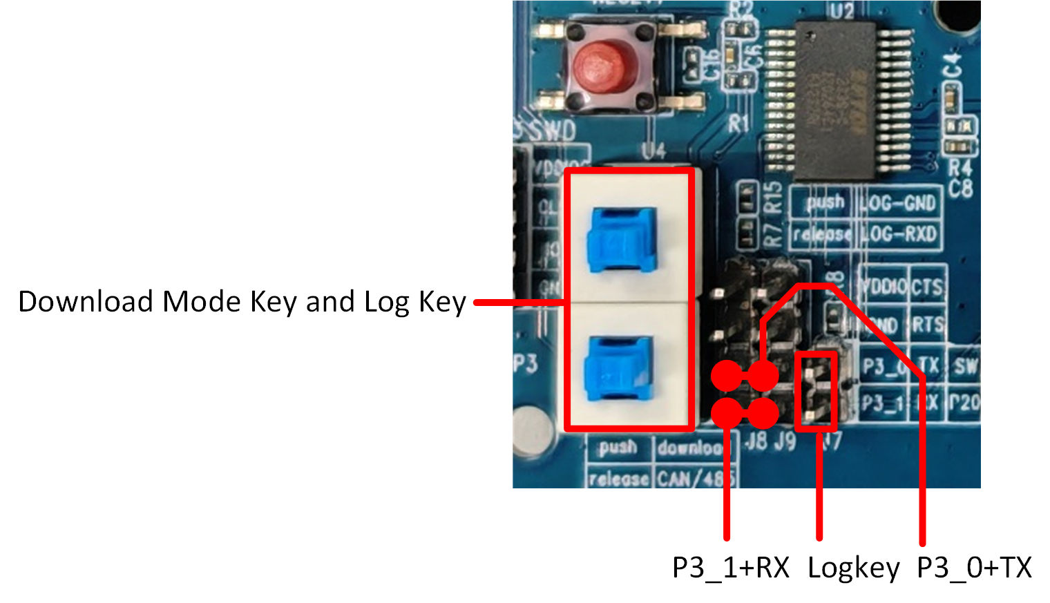
Press both button switches marked with the red box in the UART/LOG test interface diagram. In this way, P2_0 (log) will be pulled low, while P3_0 is connected to the FT232 TXD and P3_1 is connected to the FT232 RXD. Then, press the reset button or power the board off and on again to enter download mode, as shown in figure.
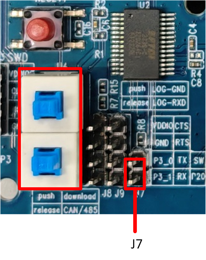
Important: After downloading the program, make sure to release both button switches. Then, power on the board again or perform a hardware reset to run the flash code. After releasing the switches, if J7 remains connected, you can use the onboard FT232 to check the log. If you want to use an external FT232 converter to read the log, you need to remove J7 and connect P2_0 to the RXD pin of the external USB-to-UART converter.
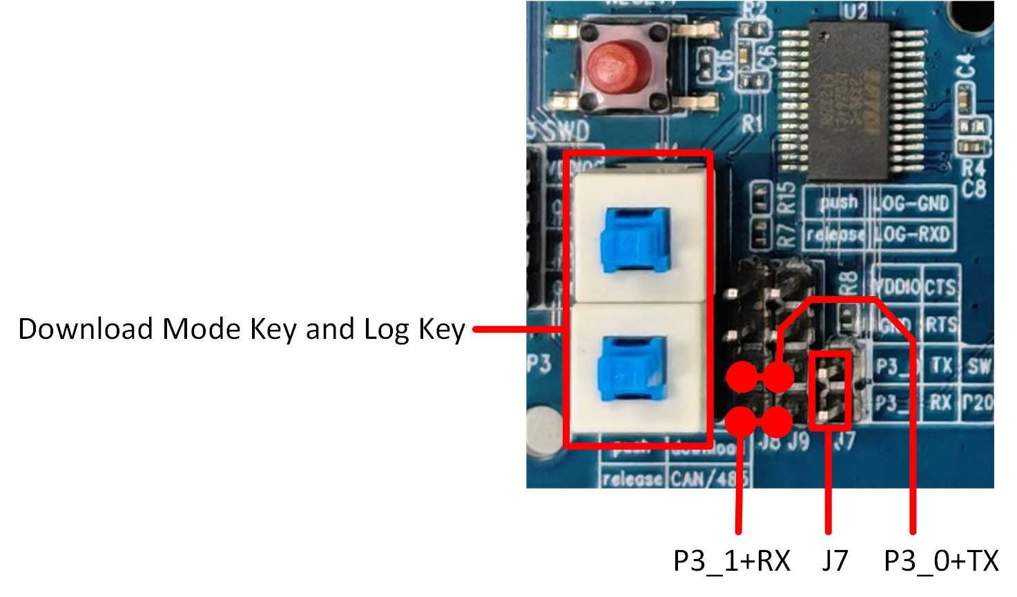
Download Mode Connection Diagram
-
SOC Mode Connection
Please make sure that the two button switches highlighted by the red boxes in the UART/LOG test interface diagram are released, and that the jumper is placed on J7. At this time, P2_0 (log) will be connected to FT232 RXD, and P3_0 and P3_1 will be disconnected from FT232 TXD and RXD, respectively. Afterwards, establish a connection to the onboard USB-to-UART chip via USB port CON2, and perform debugging using the Debug Analyzer, as shown in figure.
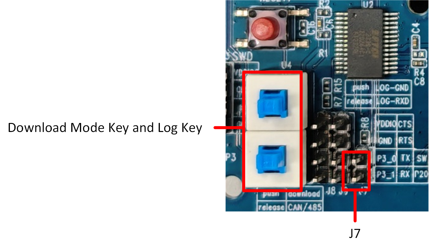
SOC Mode Connection Diagram
-
-
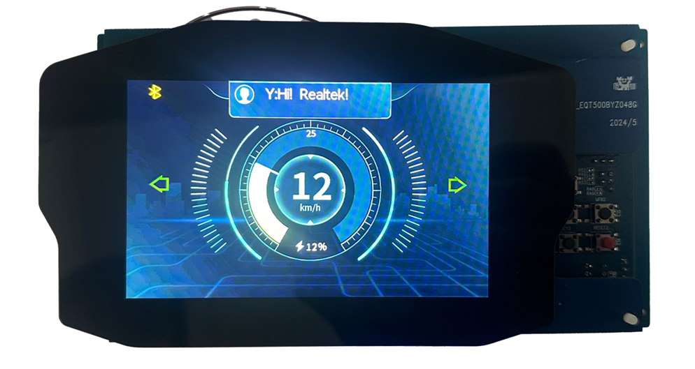
LCD Interface
The screen can be powered by USB Port CON2, CON1, or a lithium battery. If the screen’s backlight current exceeds the lithium battery’s output capability, it is recommended to use the only an external 5V power supply. For example, for the 5-inch RGB888 screen shown below, the backlight requires 1.8W of power, so it is recommended to supply power to the screen via the USB port. The RGB888 screen is shown in the following figure:
-
RF Test
When performing Bluetooth RF performance testing with the RF Test Tool, both button switches marked by the red rectangles need to be pressed. Then, remove the jumper cap from J7 to leave P2_0 floating, while P3_0 connects to TX and P3_1 connects to RX, as shown in figure.
RF Test Connection Diagram
EVB Blocks and Interfaces Introduction
Here is an introduction to the usage and tips of blocks and interfaces on RTL8773EWP evaluation board.
-
EVB Daughter Board
The EVB daughter board is removable and replaceable. The connector between the mother board and the daughter board features a reverse-insertion prevention mechanism.
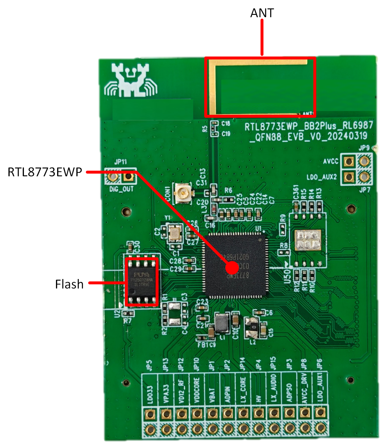
RTL8773EWP Daughter Board
-
Power
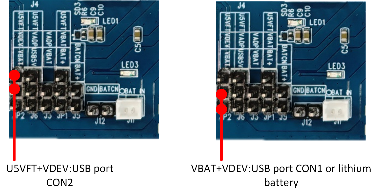
USB port CON1 is used to supply power to the RTL8773EWP evaluation board. This port does not support data communication. If this port is used for power supply, you can choose to connect USB_5V directly to VBAT. If the built-in charging function is used, connect USB_5V to VADP, and connect VBAT according to the lithium battery power supply method. USB port CON2 is used to supply power to the RTL8773EWP evaluation board and is also connected to the USB-to-UART chip FT232RL for images downloading or debugging. The RTL8773EWP evaluation board also supports lithium battery power supply. After connecting a lithium battery to J11 or J12, use a jumper to connect the pin header within the red box, as shown in figure.
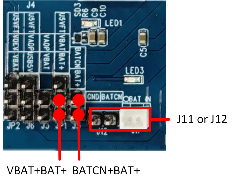
Lithium Battery Power Supply Connection Diagram
-
Evaluation Board Interface
-
UART/LOG Test Interface
-
Download mode:
Both push-button switches marked by the red box need to be pressed, and J7 must be connected. Press the reset button (or re-power the board) to enter download mode.
-
SOC/APP mode:
Both push-button switches marked by the red box need to be released, and J7 must be connected. Press the reset button (or re-power the board) to start program execution. At this time, the Log pin can be used for debugging.
-
UART LOG Test Interface Diagram
-
RS485 Interface
When using RS485, the three groups of pin headers marked in the diagram must be shorted with jumpers. The RS485 module accepts 3.3V TTL inputs. When connecting the RS485 module to the evaluation board, ensure that each pin on the module corresponds exactly to the RS485 interface pins on the evaluation board to prevent reverse connection.
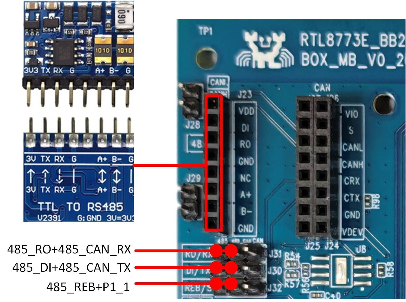
RS485 Test Interface and Module Diagram
-
A2C Interface
The A2C interface is shown in the two red boxes in the diagram: one row is for connecting the transceiver module, and the other row serves as the A2C test interface. When using the A2C interface, the three groups of pin headers marked in the diagram must be shorted with jumpers. The module uses the TJA1051 high-speed transceiver, which provides differential transmit and receive functions for the controller and supports data rates up to 1 Mbit/s. When connecting the transceiver module to the evaluation board, ensure that each pin of the module corresponds exactly to the A2C interface pins on the evaluation board to avoid reversed connections.
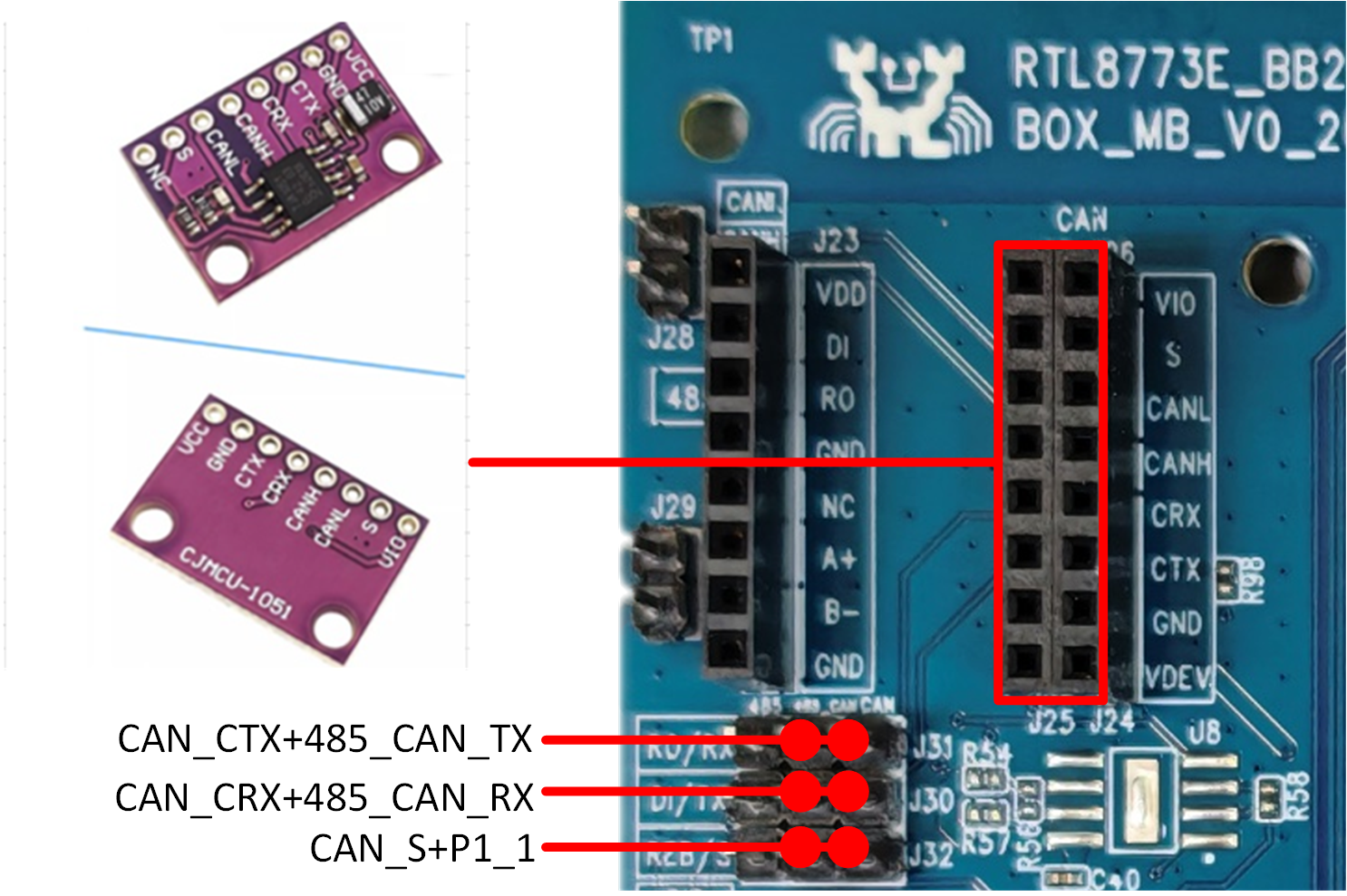
A2C Test Interface and Module Diagram
-
Infrared Sensing Interface
To use the infrared sensor module, first short J21 with a jumper cap. Then insert the infrared sensor module into J20. Pay close attention to the insertion orientation to prevent reverse connection. The infrared sensor module uses the HC-SR505, which operates at a voltage range of 4.5–20V and has a static current of less than 50μA. When a person enters the detection range, the module outputs a high level. When no one is detected, it automatically delays and then switches the output to low level. The module supports repeatable triggering: after the output goes high, if the sensor continues to detect movement within its range during the delay period, the output remains high. Only when no movement is detected will the output switch to low level after the delay.
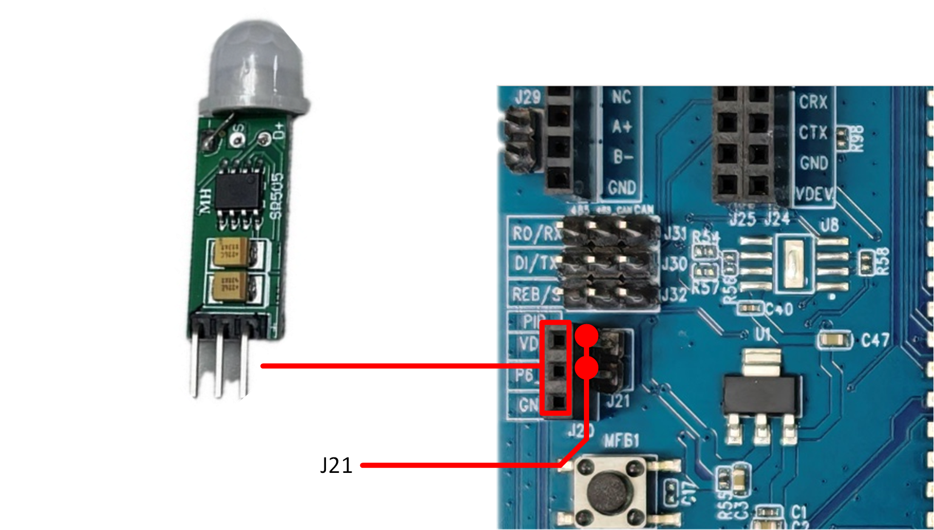
Infrared Sensing Interface and Module Diagram
-
Temperature and Humidity Sensor Interface
The temperature and humidity sensor module operates with a supply voltage of 2.4–5.5V. It supports the I2C communication protocol. Temperature range and accuracy: -40°C to +125°C, with ±0.2°C accuracy. Humidity range and accuracy: 0–100% RH, with ±2% RH accuracy. Power consumption is 4.8μW (at 1 sample/second). Ensure the correct insertion orientation when connecting the module to prevent reverse connection.
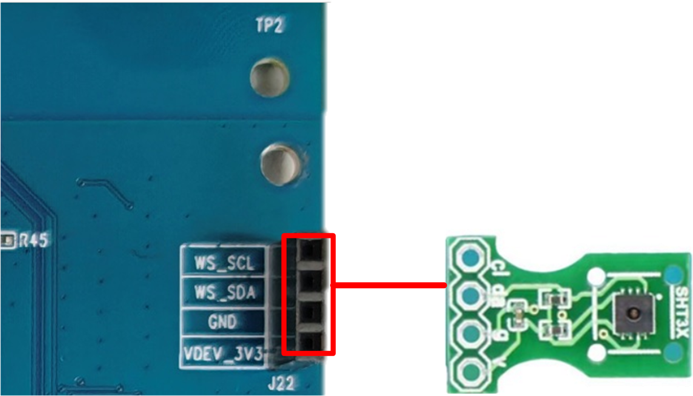
Temperature and Humidity Sensor Interface and Module Diagram
-
Wi-Fi and SD Nand Flash Multiplexed Interface
Wi-Fi Module is BL-M8189FS6, supporting SDIO interfaces. Supports the IEEE 802.11b/g/n standard and provides a PHY rate of up to 150 Mbps, providing rich wireless connectivity and reliable throughput over long distances.
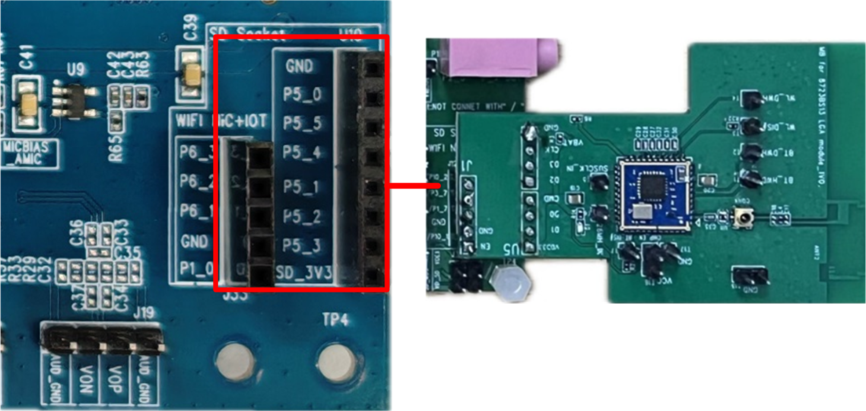
WIFI Interface and Module Diagram
-
SD Nand Flash Interface
SD Nand flash interface can be used with the RTK SD Nand flash daughterboard. When connecting, insert the SD Nand flash interface marked in the blue box on the right of figure, paying attention to the order of the connection positions to prevent reverse connection.
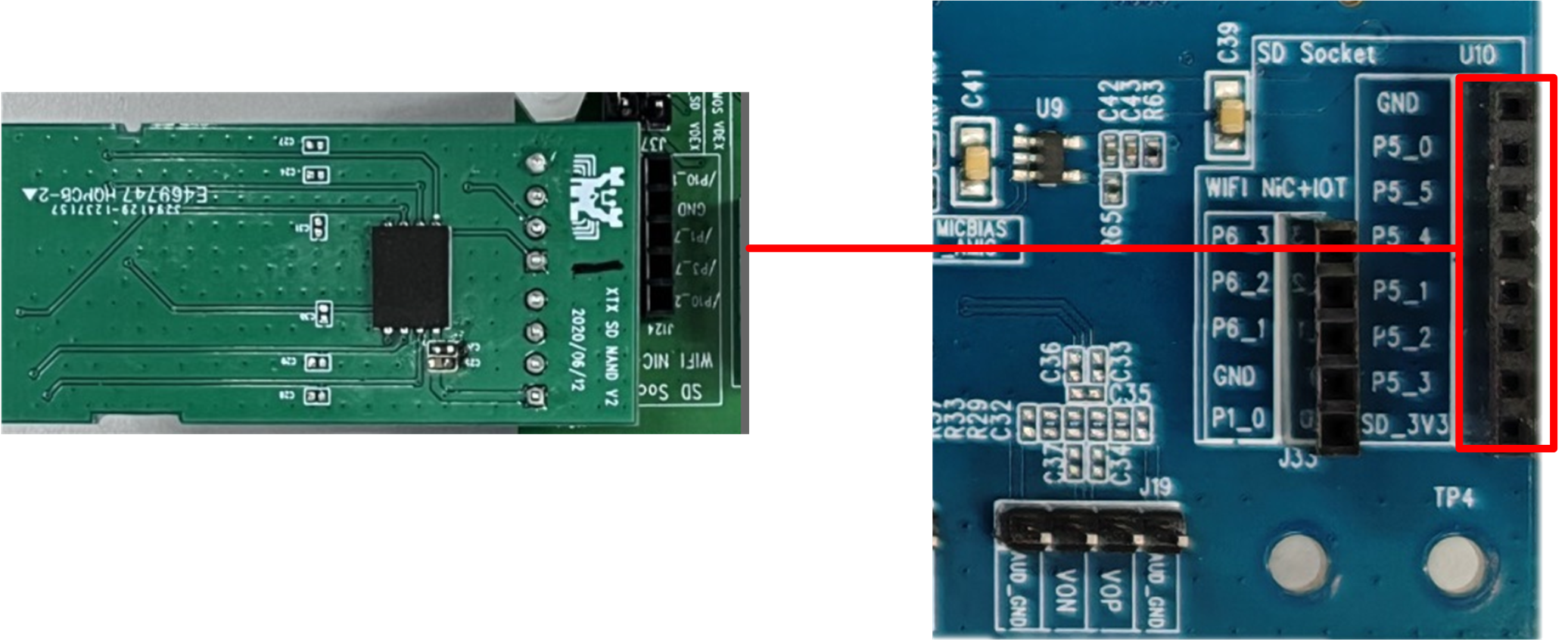
SD Nand Flash Interface and Module Diagram
Note
Normal Mode: When using the Wi-Fi or SD Nand Flash functions, pull pin P5_6 to turn on LDO U9.
Low Power Mode: If debugging low power consumption is required, pull P5_6 low before entering the chip’s low power mode to cut off power to the Wi-Fi/SD Nand Flash and prevent leakage current.
-
Speak Interface
P1 is audio codec DAC OUT interface, supporting devices with a 3.5mm audio jack. The audio output of the RTL8773EWP is Class A/B with weak driving capability and only allows loads above 10K Ohm. If 16 Ohm or 32 Ohm headphones are directly connected, the volume will decrease, and audio performance will degrade. The headphone jack can also be used with mini plug-in speakers designed for smartphones, as shown in figure. However, please note that most small speakers on the market are single-ended input. This connection method means the negative side of the RTL8773EWP differential output is left floating, resulting in poor anti-interference capability and possible introduction of pop noise.
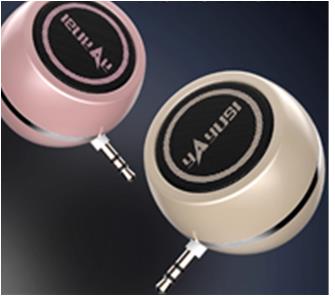
Small Speaker Diagram
-
AMIC Interface
P2 and P3 are for MIC1 and MIC2, and the power supply source for the microphones can be selected from J15. MICBIAS_AMIC provides power to AMIC (P2 and P3), and the power supply can be selected between the chip’s MICBIAS or the external LDO VMIC_1V8. J16 and J17 are pin headers for MIC1 and MIC2, which are used to connect MIC daughter boards. The MIC daughter boards must include their own bias and power supply circuits. For MEMS MIC daughter boards provided by RTK (as shown in figure), the motherboard side should connect to MIC_N, and the daughter board side should connect to MIC+N+C. The same connection method should be used for the MIC_P terminal.
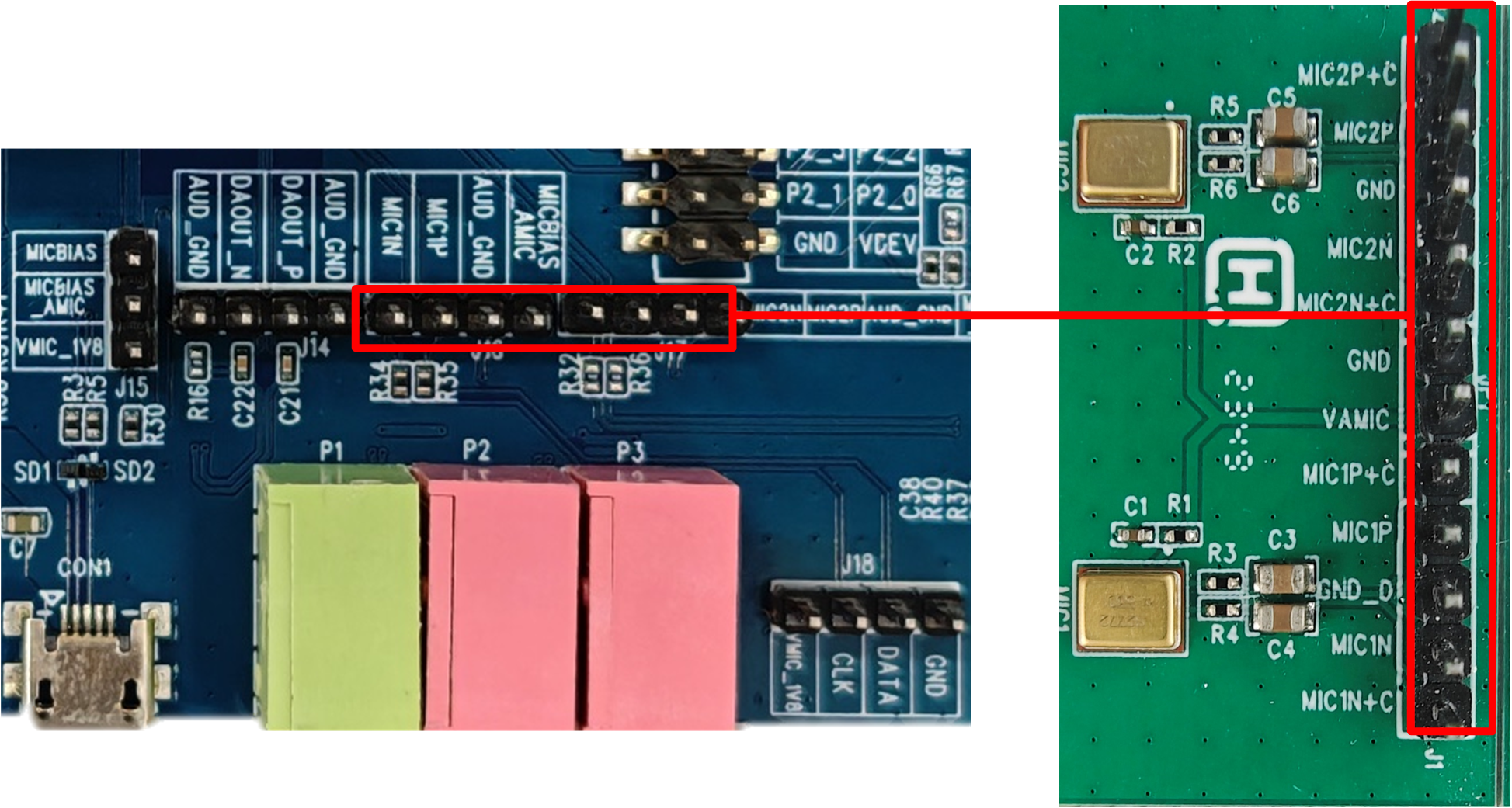
AMIC Interface and Module Diagram
-
DMIC Interface
DMICA DAT and CLK can be assigned to any pin through MCUConfigTool. If you use J18 to connect the DMIC, you need to assign MIC1_P to DMIC_DATA and MIC1_N to DMIC_CLK. The jumper connection method is shown in the figure below.
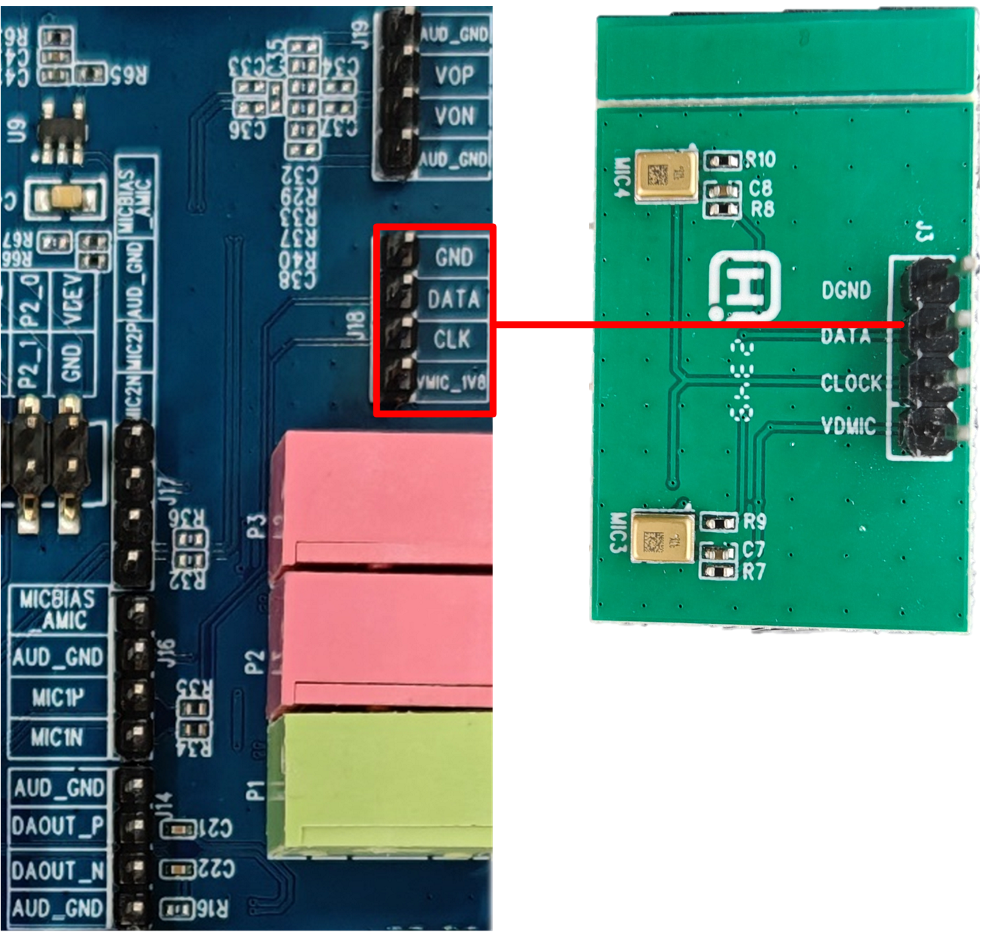
DMIC Interface and Module Diagram
-