SPI Master DLPS
This document introduces two SPI communication samples. The sample1 demonstrates how SPI master sends data by GDMA mode in DLPS situation, which wakes up the system using a software timer. The sample2 demonstrates how SPI sends and reads data by polling in DLPS situation, which wakes up the system using a wake-up pin. In both examples, SPI is configured as a master, and the direction is full-duplex. The chip sends data to the SPI slave.
Requirements
For hardware requirements, please refer to the Requirements.
Wiring
Sample 1 Wiring
Connect P2_1 (master SCK) to SCK of SPI slave device, connect P2_2 (master MOSI) to MOSI of SPI slave device, connect P2_3 (master MISO) to MISO of SPI slave device, and connect P0_1 (master CS) to CS of SPI slave device. The hardware connection of SPI sample code is shown in the figure below.
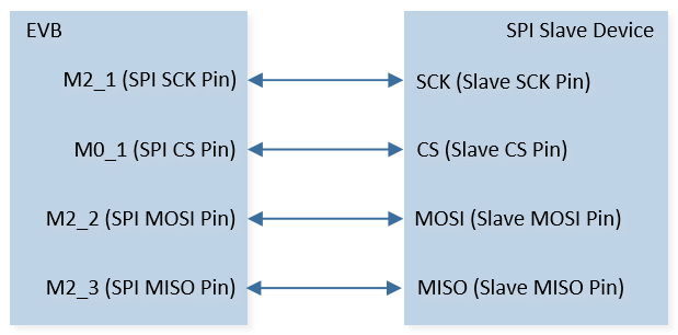
SPI Sample Code Hardware Connection Diagram
Sample 2 Wiring
Connect P1_2 (master SCK) to SCK of SPI slave device, connect P1_3 (master MOSI) to MOSI of SPI slave device, connect P1_4 (master MISO) to MISO of SPI slave device, and connect P1_5 (master CS) to CS of SPI slave device. The hardware connection of SPI sample code is shown in the figure below.
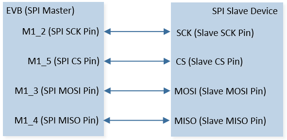
SPI Sample Code Hardware Connection Diagram
Configurations
The following macros can be configured to modify pin definitions for sample1.
#define SPI0_SCK P2_1#define SPI0_MOSI P2_2#define SPI0_MISO P2_3#define SPI0_CS P0_1
The following macros can be configured to modify pin definitions for sample2.
#define PIN_SPI0_SCK P1_2#define PIN_SPI0_MOSI P1_3#define PIN_SPI0_MISO P1_4#define PIN_SPI0_CS P1_5#define WAKE_UP_PIN P0_0
The entry function are as follows, call this function in
main()to run this sample code. For more details, please refer to the Initialization.For sample 1, use the following entry function:
spi_master_tx_dma_dlps_demo();
For sample 2, use the following entry function:
spi_dlps_demo();
Building and Downloading
For building and downloading, please refer to the Building and Downloading.
Experimental Verification
Sample 1 Verification
Press the Reset button on the EVB, the device enters DLPS and prints log.
spi_dlps_enterAfter being awakened by the timer every 1 second, the data in the array
SPI_TX_Bufis sent to SPI slave device. When completing the transmission, it enters the GDMA interrupt and prints log.spi_dlps_exit timer_callback spi_master_tx_dma_handler! tx_len_all 1000
When SPI TX FIFO level is equal to or below its threshold value, trigger the
SPI_INT_TXEinterrupt and prints log. Then the chip can enter DLPS again.spi_tx_handler: SPI TX FIFO Empty
Sample 2 Verification
Press the Reset button on the EVB.
The data in the array
SPI_WriteBufis sent to SPI slave device. If the slave device sends the same data to the chip, the chip stores the received data in arraySPI_ReadBufand prints the data in Debug Analyzer.SPI_DemoCode: SPI_ReadBuf[0] 0x9f SPI_DemoCode: SPI_ReadBuf[1] 0x2 SPI_DemoCode: SPI_ReadBuf[2] 0x0 SPI_DemoCode: SPI_ReadBuf[3] 0x0
After the transmission is complete, the system is in idle state, it will enter DLPS mode. Observe the entering DLPS message displayed in the Debug Analyzer.
DlpsEnterCallback: enter dlps
Pull down the wake-up pin to wake up the system. Observe the exiting DLPS message displayed in the Debug Analyzer.
DlpsExitCallbackAfter exiting DLPS, enter the system wake up event, then print the SPI regiter and repeat the step2 to write and read data.
Code Overview
Source Code Directory
For both samples, please refer to the Source Code Directory for the project directory.
Sample 1 source code:
Source code directory:
sdk\src\sample\io_demo\spi\dlps\spi_master_tx_dma_dlps_demo.c.
Sample 2 source code:
Source code directory:
sdk\src\sample\io_demo\spi\dlps\spi_dlps_demo.c.
DLPS Mode Initialization (Sample 1)
Call
io_dlps_register()to initialize IO store/restore and do not need to worry about which IO peripheral requires specific handling.Call
power_check_cb_register()to register inquiry callback function to DLPS framework. This function will be called each time before entering DLPS to decide whether DLPS is allowed to enter. DLPS will be disallowed if any inquiry callback function returns false. Functionio_dlps_checkwill be executed before entering DLPS.Call
io_dlps_register_enter_cb()to register callbacks to DLPS enter stage. Functionspi_dlps_enterwill be executed while entering DLPS.Call
io_dlps_register_exit_cb()to register callbacks to DLPS exit stage. Functionspi_dlps_exitwill be executed while exiting from DLPS:Set
allowedSystemEnterDlpsto false to not allow the system to enter DLPS mode.Call
spi_master_tx_dma_initto reinitialize the GDMA peripheral.
Call
bt_power_mode_set()to set Bluetooth MAC deep sleep mode.Call
power_mode_set()to switch the system to DLPS mode.
Software Timer Initialization (Sample 1)
Call
os_timer_create()to create a software timer with a period value of 1 seconds and reload mode.Call
os_timer_start()to start the software timer after setting the system to DLPS mode.
SPI TX DMA Initialization Flow (Sample 1)
The initialization flow for peripherals can refer to Initialization Flow.
The SPI TX DMA initialization flow requires first initializing the SPI peripheral, followed by TX DMA initialization.
SPI Initialization Flow
The SPI initialization flow can refer to SPI Initialization Flow Chart.
Call
Pad_Config()andPinmux_Config()to initialize the pin.static void board_spi_init(void) { Pinmux_Config(SPI0_SCK, SPI0_CLK_MASTER); Pinmux_Config(SPI0_MOSI, SPI0_MO_MASTER); Pinmux_Config(SPI0_MISO, SPI0_MI_MASTER); Pinmux_Config(SPI0_CS, SPI0_SS_N_0_MASTER); Pad_Config(SPI0_SCK, PAD_PINMUX_MODE, PAD_IS_PWRON, PAD_PULL_NONE, PAD_OUT_DISABLE, PAD_OUT_HIGH); Pad_Config(SPI0_MOSI, PAD_PINMUX_MODE, PAD_IS_PWRON, PAD_PULL_NONE, PAD_OUT_DISABLE, PAD_OUT_HIGH); Pad_Config(SPI0_MISO, PAD_PINMUX_MODE, PAD_IS_PWRON, PAD_PULL_NONE, PAD_OUT_DISABLE, PAD_OUT_HIGH); Pad_Config(SPI0_CS, PAD_PINMUX_MODE, PAD_IS_PWRON, PAD_PULL_NONE, PAD_OUT_DISABLE, PAD_OUT_HIGH); }
Call
RCC_PeriphClockCmd()to enable the SPI clock and function.Initialize the SPI peripheral:
Define the
SPI_InitTypeDeftypeSPI_InitStructure, and callSPI_StructInit()to pre-fillSPI_InitStructurewith default values.Modify the
SPI_InitStructureparameters as needed. The SPI initialization parameter configuration is shown in the table below.Call
SPI_Init()to initialize the SPI peripheral,SPI0_HSis seleted.
SPI Initialization Parameters SPI Hardware Parameters
Setting in the
SPI_InitStructureSPI
Direction
Device Role (SPI Master or SPI Slave)
Data Frame Size
Clock Polarity
Clock Phase
Clock Div
100
Frame Format
Transmit FIFO Threshold Level
0
RX Water Level
7
Call
RamVectorTableUpdate()to register the SPI interrupt handler.Call
SPI_Cmd()to enable SPI.
TX DMA Initialization Flow
The SPI TX DMA initialization flow can refer to SPI TX DMA Initialization Flow Chart.
Call
GDMA_channel_requestto request a free GDMA channel and register the GDMA interrupt handler.Call
RCC_PeriphClockCmd()to enable the GDMA clock and function.Initialize the GDMA peripheral:
Define the
GDMA_InitTypeDeftypeGDMA_InitStruct, and callGDMA_StructInit()to pre-fillGDMA_InitStructwith default values.Modify the
GDMA_InitStructparameters as needed. The GDMA initialization parameter configuration is shown in the table below.Call
GDMA_Init()to initialize the GDMA peripheral.
GDMA Initialization Parameters GDMA Hardware Parameters
Setting in the
GDMA_InitStructGDMA
Channel Num
SPI_MASTER_TX_DMA_CHANNEL_NUMTransfer Direction
Buffer Size
SPI_DATA_LENSource Address Increment or Decrement
Destination Address Increment or Decrement
Source Data Size
Destination Data Size
Source Burst Transaction Length
Destination Burst Transaction Length
Source Address
SPI_TX_BufDestination Address
SPI0->DRDestination Handshake
GDMA_Handshake_SPI0_TXCall
GDMA_INTConfig()to enable TX GDMA transfer complete interruptGDMA_INT_Transfer.Call
NVIC_Init()to enable NVIC of TX GDMA.
DLPS Mode Initialization (Sample 2)
Call
io_dlps_register()to initialize IO store/restore and do not need to worry about which IO peripheral requires specific handling.Call
io_dlps_register_enter_cb()to register callbacks to DLPS enter stage. FunctionDlpsEnterCallbackwill be executed while entering DLPS:Call
Pad_PullUpOrDownValue()to configWAKE_UP_PINpull up.Call
System_WakeUpPinEnable()to enable the wake-up function ofWAKE_UP_PIN.
Call
io_dlps_register_exit_cb()to register callbacks to DLPS exit stage. FunctionDlpsExitCallbackwill be executed while exiting from DLPS.Call
bt_power_mode_set()to set Bluetooth MAC deep sleep mode.Call
power_mode_set()to switch the system to DLPS mode.
SPI TX Initialization (Sample 2)
The initialization flow for peripherals can refer to Initialization Flow. More details please refer to TX Polling Initialization Flow.
Functional Implementation
Software Timer Callback Handle (Sample 1)
When the software timer expires, the software timer callback function will be executed:
Call
SPI_GDMACmd()to disable and then enable SPI GDMA TX Function.Call
GDMA_Cmd()to enable TX DMA transfers.Call
SPI_INTConfig()to enable TX FIFO empty interruptSPI_INT_TXE.
SPI TX DMA Interrupt Handle (Sample 1)
When GDMA transfer is completed, transfer complete interrupt is triggered:
Call
GDMA_GetTransferLen()to get the GDMA transfer data length.Call
GDMA_INTConfig()to disable GDMA transfer complete interruptGDMA_INT_Transfer.Call
GDMA_ClearINTPendingBit()to clearGDMA_INT_Transferinterrupt.Call
GDMA_INTConfig()to enable GDMA transfer complete interruptGDMA_INT_Transferfor next transmission.
SPI TX Interrupt Handle (Sample 1)
When the transmit buffer reaches or goes below the TX FIFO threshold level (SPI_InitTypeDef::SPI_TxThresholdLevel),
TX FIFO empty interrupt will be triggered and enters the interrupt handler:
Call
SPI_GetINTStatus()to checkSPI_INT_TXEinterrupt status.Call
SPI_INTConfig()to disableSPI_INT_TXE.Set
allowedSystemEnterDlpsto true to allow the system to enter DLPS mode.
Send and Receive Data by Polling (Sample 2)
Call
SPI_SendBuffer()to send the data inSPI_WriteBufto the slave.Call
SPI_GetFlagState()to checkSPI_FLAG_BUSYflag state, and wait for the SPI data transfer to complete.Call
SPI_GetRxFIFOLen()to get the data length in RX FIFO.Call
SPI_ReceiveData()to receive data from RX FIFO.