SPI Slave DLPS
This document introduces two SPI communication samples. The two sample demonstrates how SPI slave receives data by GDMA mode in DLPS situation.
Sample 1 uses a GPIO pin to wake up the system. Users can wake up the system to receive data by pulling the pin high, and return to DLPS mode by pulling the pin low.
Sample 2 wakes up the system using the SPI CS pin, CS pin will pull low when master device sends data. And add software timer to allow system enter DLPS. It should be noted that before sending each packet of data, the master needs to send an extra dummy data to wake up the slave. Since the wake-up takes time, the data used for wake-up will be lost.
In both examples, SPI is configured as a slave, and the direction is full-duplex. The chip reads data from the master when exit DLPS.
Requirements
For hardware requirements, please refer to the Requirements.
Wiring
Connect P2_1 (slave SCK) to SCK of SPI master device, connect P2_2 (slave MOSI) to MOSI of SPI master device, connect P2_3 (slave MISO) to MISO of SPI master device, and connect P0_1 (slave CS) to CS of SPI master device. The hardware connection of SPI sample code is shown in the figure below.
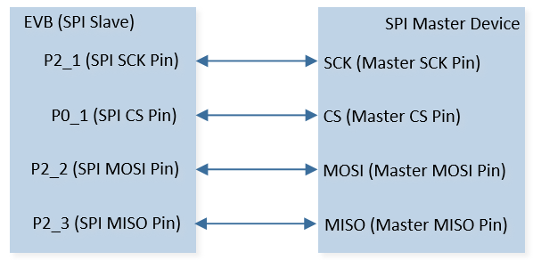
SPI Sample Code Hardware Connection Diagram
Configurations
The following macros can be configured to modify pin definitions.
#define PIN_SPI_SCK P2_1#define PIN_SPI_MOSI P2_2#define PIN_SPI_MISO P2_3#define PIN_SPI_CS P0_1
The entry function are as follows, call this function in
main()to run this sample code. For more details, please refer to the Initialization.For sample 1, use the following entry function:
spi_dlps_slave_rx_dma_gpio_demo();
For sample 2, use the following entry function:
spi_dlps_slave_rx_dma_demo();
Building and Downloading
For building and downloading, please refer to the Building and Downloading.
Experimental Verification
Sample 1 Verification
Press the Reset button on the EVB.
After initialization is complete, the system is in idle state, it will enter DLPS mode. Observe the entering DLPS message displayed in the Debug Analyzer.
spi_dlps_enterPull up the wake-up pin to wake up the system. Observe the exiting DLPS message displayed in the Debug Analyzer.
spi_dlps_exitEnter gpio interrupt and send message to enable DMA receive data. Once the SPI receives the data, it will print the following message in the Debug Analyzer.
spi_slave_gpio_cb: gpio_level 1
spi_slave_rx_dma_handler! rx_len_all 6
spi_slave_rx_dma_handler: read_buf[0] = 0x%x
...
spi_slave_rx_dma_handler: read_buf[5] = 0x%x
Pull down the wake-up pin to allow the system re-enter DLPS mode.
spi_slave_gpio_cb: gpio_level 0
spi_dlps_enter
Sample 2 Verification
Press the Reset button on the EVB.
After initialization is complete, the system is in idle state, it will enter DLPS mode. Observe the entering DLPS message displayed in the Debug Analyzer.
spi_dlps_enterWhen the master sends data, CS is pulled low and the system will be awakened. Observe the exiting DLPS message displayed in the Debug Analyzer.
spi_dlps_exitAfter exiting dlps, slave enables DMA to receive data. When completing the transmission, it enters the GDMA interrupt and prints log.
spi_slave_rx_dma_handler! rx_len_all 6
spi_slave_rx_dma_handler: read_buf[0] = 0x%x
...
spi_slave_rx_dma_handler: read_buf[5] = 0x%x
When the software timer expires, the system is allowed to re-enter DLPS mode.
timer_callback
Code Overview
Source Code Directory
For both samples, please refer to the Source Code Directory for the project directory.
Sample 1 source code:
Source code directory:
sdk\src\sample\io_demo\spi\dlps\spi_dlps_slave_rx_dma_gpio_demo.c.
Sample 2 source code:
Source code directory:
sdk\src\sample\io_demo\spi\dlps\spi_dlps_slave_rx_dma_demo.c.
DLPS Mode Initialization (Sample 1)
Call
io_dlps_register()to initialize IO store/restore and do not need to worry about which IO peripheral requires specific handling.Call
power_check_cb_register()to register inquiry callback function to DLPS framework. This function will be called each time before entering DLPS to decide whether DLPS is allowed to enter. DLPS will be disallowed if any inquiry callback function returns false. Functionio_dlps_checkwill be executed before entering DLPS.Call
io_dlps_register_enter_cb()to register callbacks to DLPS enter stage. Functionspi_dlps_enterwill be executed while entering DLPS:Call
System_WakeUpPinEnable()to to enable the wake-up function ofPIN_GPIO_WAKEUP.
Call
io_dlps_register_exit_cb()to register callbacks to DLPS exit stage. Functionspi_dlps_exitwill be executed while exiting from DLPS:Call
System_WakeUpInterruptValue()to check if the wake-up was triggered by thePIN_GPIO_WAKEUP.If the wake-up was triggered by the current
PIN_GPIO_WAKEUP, call the interrupt function of the GPIO.Then set
allowedSystemEnterDlpsto false to not allow the system to enter DLPS mode.Then call
spi_slave_rx_dma_initto reinitialize the GDMA peripheral, and callspi_dma_rx_datato enable receive data.
Call
bt_power_mode_set()to set Bluetooth MAC deep sleep mode.Call
power_mode_set()to switch the system to DLPS mode.
GPIO Interrupt Initialization (Sample 1)
Call
hal_gpio_init()to enable GPIO clock.Call
hal_gpio_int_init()to initialize GPIO interrupt.Call
hal_gpio_set_debounce_time()to set GPIO debounce time.Call
hal_gpio_init_pin()to initialize the GPIO peripheral and callhal_gpio_set_up_irq()to initialize interrupt-related parameters. The GPIO initialization parameters are configured as shown in the table below.
GPIO Hardware Parameters |
GPIO |
|---|---|
PIN Number |
|
GPIO Type |
|
GPIO Mode |
|
GPIO Pull Value |
|
Interrupt Type |
|
Interrupt Polarity |
|
Debounce Enable |
|
Call
hal_gpio_register_isr_callback()to register gpio interrupt callback.Call
hal_gpio_irq_enable()to enable gpio interrupt.
SPI RX DMA Initialization Flow (Sample 1&2)
The initialization flow for peripherals can refer to Initialization Flow.
The SPI RX DMA initialization flow requires first initializing the SPI peripheral, followed by RX DMA initialization.
SPI Initialization Flow
The SPI initialization flow can refer to SPI Initialization Flow Chart.
Call
Pad_Config()andPinmux_Config()to initialize the pin.static void board_spi_init(void) { Pinmux_Config(PIN_SPI_SCK, SPI_CLK_SLAVE); Pinmux_Config(PIN_SPI_MOSI, SPI_MO_SLAVE); Pinmux_Config(PIN_SPI_MISO, SPI_MI_SLAVE); Pinmux_Config(PIN_SPI_CS, SPI_SS_N_0_SLAVE); Pad_Config(PIN_SPI_SCK, PAD_PINMUX_MODE, PAD_IS_PWRON, PAD_PULL_NONE, PAD_OUT_DISABLE, PAD_OUT_HIGH); Pad_Config(PIN_SPI_MOSI, PAD_PINMUX_MODE, PAD_IS_PWRON, PAD_PULL_NONE, PAD_OUT_DISABLE, PAD_OUT_HIGH); Pad_Config(PIN_SPI_MISO, PAD_PINMUX_MODE, PAD_IS_PWRON, PAD_PULL_NONE, PAD_OUT_DISABLE, PAD_OUT_HIGH); Pad_Config(PIN_SPI_CS, PAD_PINMUX_MODE, PAD_IS_PWRON, PAD_PULL_NONE, PAD_OUT_DISABLE, PAD_OUT_HIGH); }
Call
RCC_PeriphClockCmd()to enable the SPI clock and function.Initialize the SPI peripheral:
Define the
SPI_InitTypeDeftypeSPI_InitStructure, and callSPI_StructInit()to pre-fillSPI_InitStructurewith default values.Modify the
SPI_InitStructureparameters as needed. The SPI initialization parameter configuration is shown in the table below.Call
SPI_Init()to initialize the SPI peripheral,SPI0_HSis seleted.
SPI Initialization Parameters SPI Hardware Parameters
Setting in the
SPI_InitStructureSPI
Direction
Device Role (SPI Master or SPI Slave)
Data Frame Size
Clock Polarity
Clock Phase
RX Water Level
7
Call
SPI_Cmd()to enable SPI.
RX DMA Initialization Flow
The SPI RX DMA initialization flow can refer to SPI RX DMA Initialization Flow Chart.
Call
GDMA_channel_requestto request a free GDMA channel and register the GDMA interrupt handler.Call
RCC_PeriphClockCmd()to enable the GDMA clock and function.Initialize the GDMA peripheral:
Define the
GDMA_InitTypeDeftypeGDMA_InitStruct, and callGDMA_StructInit()to pre-fillGDMA_InitStructwith default values.Modify the
GDMA_InitStructparameters as needed. The GDMA initialization parameter configuration is shown in the table below.Call
GDMA_Init()to initialize the GDMA peripheral.
GDMA Initialization Parameters GDMA Hardware Parameters
Setting in the
GDMA_InitStructGDMA
Channel Num
SPI_SLAVE_RX_DMA_CHANNEL_NUMTransfer Direction
Buffer Size
TEST_SIZESource Address Increment or Decrement
Destination Address Increment or Decrement
Source Data Size
Destination Data Size
Source Burst Transaction Length
Destination Burst Transaction Length
Source Address
SPI0->DRDestination Address
read_bufSource Handshake
DMA_Handshake_SPI_SLAVE_RXCall
GDMA_INTConfig()to enable RX GDMA transfer complete interruptGDMA_INT_Transfer.Call
NVIC_Init()to enable NVIC of RX GDMA.
DLPS Mode Initialization (Sample 2)
Call
io_dlps_register()to initialize IO store/restore and do not need to worry about which IO peripheral requires specific handling.Call
power_check_cb_register()to register inquiry callback function to DLPS framework. This function will be called each time before entering DLPS to decide whether DLPS is allowed to enter. DLPS will be disallowed if any inquiry callback function returns false. Functionio_dlps_checkwill be executed before entering DLPS.Call
io_dlps_register_enter_cb()to register callbacks to DLPS enter stage. Functionspi_dlps_enterwill be executed while entering DLPS:Call
Pad_PullUpOrDownValue()to configPIN_SPI_CSpull up.Call
System_WakeUpPinEnable()to enable the wake-up function ofPIN_SPI_CS.
Call
io_dlps_register_exit_cb()to register callbacks to DLPS exit stage. Functionspi_dlps_exitwill be executed while exiting from DLPS:Call
System_WakeUpInterruptValue()to check if the wake-up was triggered by thePIN_SPI_CS.Set
allowedSystemEnterDlpsto false to not allow the system to enter DLPS mode, and start the software timer.Call
spi_slave_rx_dma_initto reinitialize the GDMA peripheral, and callspi_dma_rx_datato enable receive data.
Call
bt_power_mode_set()to set Bluetooth MAC deep sleep mode.Call
power_mode_set()to switch the system to DLPS mode.
Software Timer Initialization (Sample 2)
Call
os_timer_create()to create a software timer with a period value of 500 ms and reload mode.Call
os_timer_start()to start the software timer after exiting from DLPS mode.
Functional Implementation
GPIO Interrupt Handle (Sample 1)
The interrupt handler function spi_slave_gpio_cb prints interrupt information.
When detecting a high level of P1_1 triggers a GPIO interrupt. Set
allowedSystemEnterDlpsto false to not allow the system to enter DLPS mode. Then send message to enable DMA to receive data.When detecting a low level of P1_1 triggers a GPIO interrupt. Set
allowedSystemEnterDlpsto true to allow the system to enter DLPS mode.
static void spi_slave_gpio_cb(uint32_t context)
{
   uint8_t pin_index = (uint32_t)context;
   uint8_t event = IO_DEMO_EVENT_SPI_RX;
   T_GPIO_LEVEL gpio_level = hal_gpio_get_input_level(pin_index);
   IO_PRINT_INFO1("spi_slave_gpio_cb: gpio_level %d", gpio_level);

   if (gpio_level == GPIO_LEVEL_HIGH)
   {
      allowedSystemEnterDlps = false;
      hal_gpio_irq_change_polarity(PIN_GPIO_WAKEUP, GPIO_IRQ_ACTIVE_LOW);

      if (os_msg_send(io_queue_handle, &event, 0) == false)
      {
            IO_PRINT_ERROR0("spi_slave_gpio_cb: Send Queue Error");
      }
   }
   else
   {
      allowedSystemEnterDlps = true;
      hal_gpio_irq_change_polarity(PIN_GPIO_WAKEUP, GPIO_IRQ_ACTIVE_HIGH);
   }
}
SPI RX DMA Interrupt Handle (Sample 1&2)
When GDMA transfer is completed, transfer complete interrupt is triggered:
Call
GDMA_GetTransferLen()to get the GDMA transfer data length.Call
GDMA_INTConfig()to disable GDMA transfer complete interruptGDMA_INT_Transfer.Call
GDMA_ClearINTPendingBit()to clearGDMA_INT_Transferinterrupt.
Software Timer Callback Handle (Sample 2)
When the software timer expires, the software timer callback function will be executed.
Set allowedSystemEnterDlps to true to allow the system to re-enter DLPS mode.