SPI Slave Write DMA
The sample demonstrates how SPI0 slave sends data by GDMA and receives data by interrupt. The chip sends data to the SPI master and receives data from it.
Requirements
For hardware requirements, please refer to the Requirements.
Wiring
Connect P1_0 (slave SCK) to SCK of SPI master device, connect P1_1 (slave MOSI) to MOSI of SPI master device, connect P2_1 (slave MISO) to MISO of SPI master device, and connect P2_2 (slave CS) to CS of SPI master device. The hardware connection of SPI sample code is shown in the figure below.
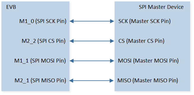
SPI Sample Code Hardware Connection Diagram
Configurations
The following macros can be configured to modify pin definitions.
#define PIN_SPI_SCK P1_0#define PIN_SPI_MOSI P1_1#define PIN_SPI_MISO P2_1#define PIN_SPI_CS P2_2
The entry function are as follows, call this function in
main()to run this sample code. For more details, please refer to the Initialization.spi_slave_write_demo();
Building and Downloading
For building and downloading, please refer to the Building and Downloading.
Experimental Verification
Press the Reset button on the EVB, the data in array
send_bufis sent to SPI TX FIFO.When master device sends data to the chip, the
send_bufcan be sent to SPI master. When completing the transmission, it enters the GDMA interrupt and prints log.spi_slave_tx_dma_handlerAnd the chip stores the received data in array
SPI_ReadINTBufand prints log in Debug Analyzer.spi_slave_handler: SPI_ReadINTBuf[0] 0x%x ... spi_slave_handler: SPI_ReadINTBuf[15] 0x%x
Code Overview
Source Code Directory
For project directory, please refer to Source Code Directory.
Source code directory:
sdk\src\sample\io_demo\spi\slave\spi_slave_write_demo.c.
SPI Initialization Flow
The initialization flow for peripherals can refer to Initialization Flow.
SPI initialization flow is shown in the following figure.
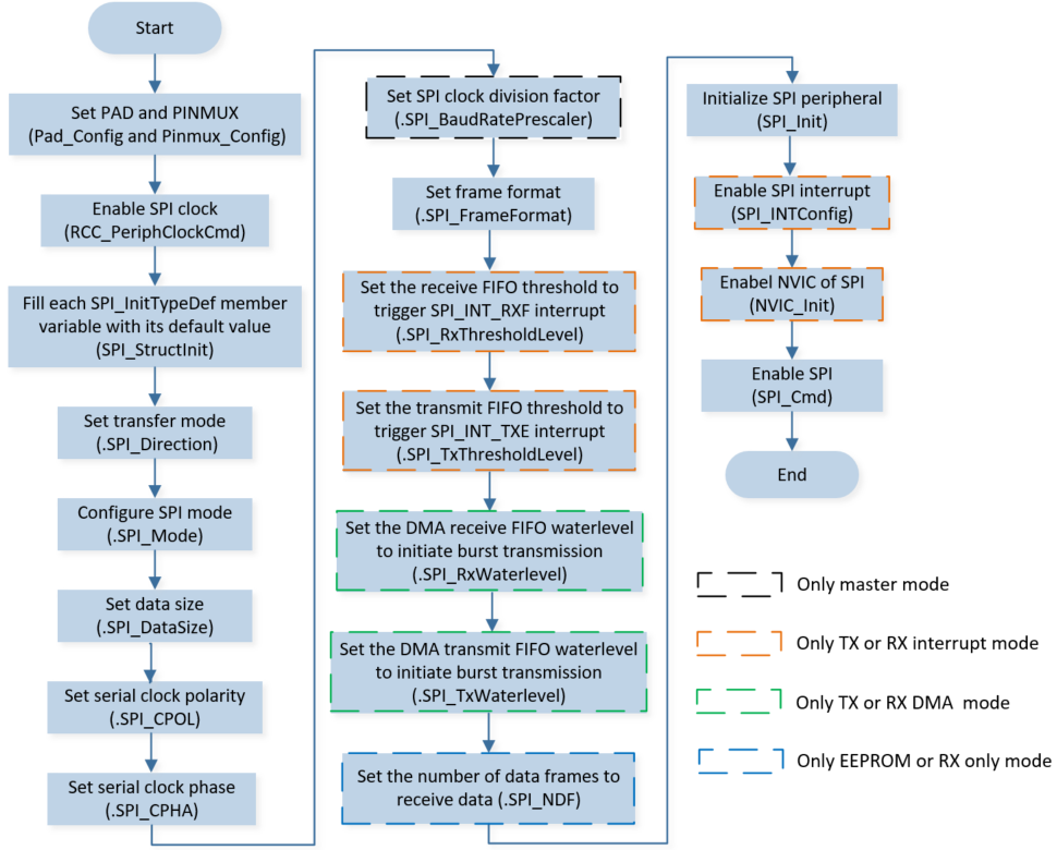
SPI Initialization Flow Chart
Call
Pad_Config()andPinmux_Config()to initialize the pins.static void board_spi_pinmux_init(void) { Pinmux_Config(PIN_SPI_SCK, SPI_CLK_SLAVE); Pinmux_Config(PIN_SPI_MOSI, SPI_MO_SLAVE); Pinmux_Config(PIN_SPI_MISO, SPI_MI_SLAVE); Pinmux_Config(PIN_SPI_CS, SPI_SS_N_0_SLAVE); Pad_Config(PIN_SPI_SCK, PAD_PINMUX_MODE, PAD_IS_PWRON, PAD_PULL_NONE, PAD_OUT_DISABLE, PAD_OUT_HIGH); Pad_Config(PIN_SPI_MOSI, PAD_PINMUX_MODE, PAD_IS_PWRON, PAD_PULL_NONE, PAD_OUT_DISABLE, PAD_OUT_HIGH); Pad_Config(PIN_SPI_MISO, PAD_PINMUX_MODE, PAD_IS_PWRON, PAD_PULL_NONE, PAD_OUT_DISABLE, PAD_OUT_HIGH); Pad_Config(PIN_SPI_CS, PAD_PINMUX_MODE, PAD_IS_PWRON, PAD_PULL_NONE, PAD_OUT_DISABLE, PAD_OUT_HIGH); }
Call
RCC_PeriphClockCmd()to enable the SPI clock and function.Initialize the SPI peripheral:
Define the
SPI_InitTypeDeftypeSPI_InitStructure, and callSPI_StructInit()to pre-fillSPI_InitStructurewith default values.Modify the
SPI_InitStructureparameters as needed. The SPI initialization parameter configuration is shown in the table below.Call
SPI_Init()to initialize the SPI peripheral.
SPI Initialization Parameters SPI Hardware Parameters
Setting in the
SPI_InitStructureSPI
Direction
Device Role (SPI Master or SPI Slave)
Data Frame Size
Clock Polarity
Clock Phase
Clock Div
100
Receive FIFO Threshold Level
0
TX Water Level
7
Call
RamVectorTableUpdate()to register SPI slave interrupt handler.Call
SPI_INTConfig()to enable RX FIFO full interruptSPI_INT_RXF.Call
NVIC_Init()to enable NVIC of SPI.Call
SPI_Cmd()to enable SPI.
TX DMA Initialization Flow
The initialization flow for peripherals can refer to Initialization Flow.
SPI TX DMA initialization flow is shown in the following figure.
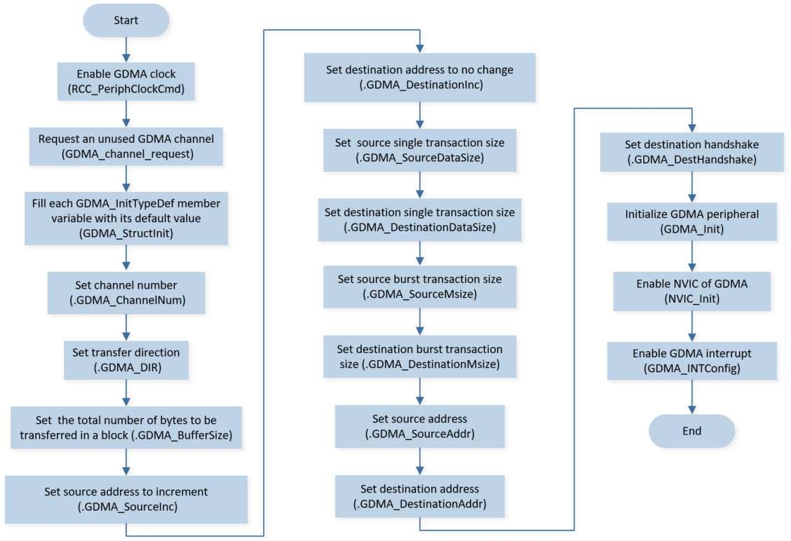
SPI TX DMA Initialization Flow Chart
Call
RCC_PeriphClockCmd()to enable the GDMA clock and function.Call
GDMA_channel_requestto request a free GDMA channel and register the GDMA interrupt handler.Initialize the GDMA peripheral:
Define the
GDMA_InitTypeDeftypeGDMA_InitStruct, and callGDMA_StructInit()to pre-fillGDMA_InitStructwith default values.Modify the
GDMA_InitStructparameters as needed. The GDMA initialization parameter configuration is shown in the table below.Call
GDMA_Init()to initialize the GDMA peripheral.
GDMA Initialization Parameters GDMA Hardware Parameters
Setting in the
GDMA_InitStructGDMA
Channel Num
SPI_SLAVE_TX_DMA_CHANNEL_NUMTransfer Direction
Buffer Size
TEST_SIZESource Address Increment or Decrement
Destination Address Increment or Decrement
Source Data Size
Destination Data Size
Source Burst Transaction Length
Destination Burst Transaction Length
Source Address
sendbufDestination Address
SPI0->DRDestination Handshake
GDMA_Handshake_SPI0_TXCall
GDMA_INTConfig()to enable GDMA transfer complete interruptGDMA_INT_Transfer.Call
NVIC_Init()to enable NVIC of GDMA.
Functional Implementation
Slave Send Data by DMA
Call
SPI_GDMACmd()to disable and then enable SPI GDMA RX Function.Call
GDMA_Cmd()to enable DMA transfers.When GDMA transfer is completed, transfer complete interrupt is triggered. Then call
GDMA_ClearINTPendingBit()to clearGDMA_INT_Transferinterrupt.
Slave Receive Data by Interrupt
Please refer to Receive Data by Interrupt.