Image Layout
This section primarily introduces Flash Layout and Image Format.
Flash Layout
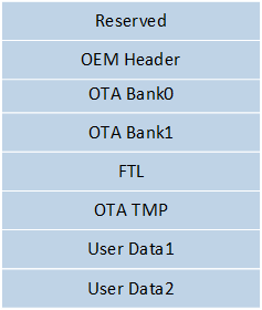
The Flash Layout of RTL8752H is as follows, consisting of Reserved, OEM Header (storage space for Config File), OTA Bank0, OTA Bank1, FTL, OTA TMP, User Data1 and User Data2. The starting address for accessing Flash is 0x00800000.
Flash Layout
Memory Segment |
Starting Address |
Size(Bytes) |
Functions |
Support DFU |
|---|---|---|---|---|
OEM Header |
0x00801000 |
0x1000 |
Storage of Config information, including Bluetooth address and Customizable Flash Layout. |
No |
OTA Bank0 |
Variable (Determined by OEM Header) |
Variable (Determined by OEM Header) |
OTA Bank0 is primarily used to store the firmware and runtime data of the device. For specific functions, refer to OTA Bank Flash Segmentation. |
Yes |
OTA Bank1 |
Variable (Determined by OEM Header) |
Variable (Determined by OEM Header) |
In the supporting Bank switching DFU scheme.
|
Yes |
FTL |
Variable (Determined by OEM Header) |
Variable (Determined by OEM Header) |
This area supports accessing flash by logical address. |
No |
OTA TMP |
Variable (Determined by OEM Header) |
Variable (Determined by OEM Header) |
If using non-supporting Bank switching DFU scheme, and instead using one bank as the backup area, then the size of the backup area must be equal to or greater than the maximum size of the image stored in OTA Bank0. |
No |
User Data1 |
Variable (Determined by OEM Header) |
Variable (Determined by OEM Header) |
The remaining space of the Flash can be used as the application's customized area. |
Yes |
User Data2 |
Variable (Determined by OEM Header) |
Variable (Determined by OEM Header) |
The remaining space of the Flash can be used as the application's customized area. |
Yes |
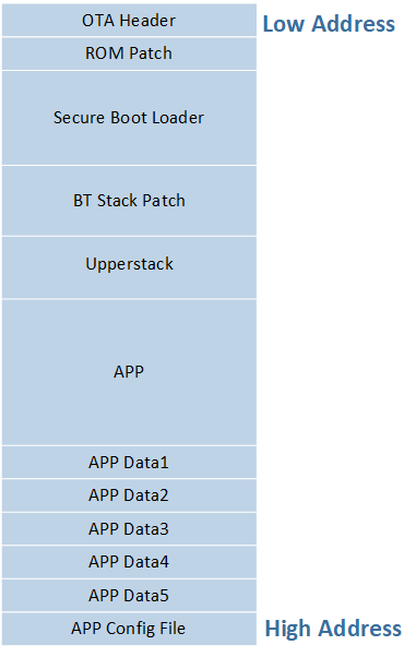
OTA Bank layout and description for each part is shown below.
Layout of OTA Bank
Memory Segment |
Starting Address |
Size(Bytes) |
Functions |
Support DFU |
|---|---|---|---|---|
OTA Header |
Determined in the OEM Header region |
4KB |
This region contains the OTA Header version and start address and size of the images in the bank. |
Yes, when using supporting Bank switching scheme. No, when using non-supporting Bank switching scheme. |
Secure Boot Loader |
Determined in the OTA Header region |
Variable |
Security check of code in boot process. |
Yes |
ROM Patch |
Determined in the OTA Header region |
Variable |
Extended function of platform features in ROM. |
Yes |
BT Stack Patch |
Determined in the OTA Header region |
Variable |
Bluetooth controller protocol stack optimization and extension code. |
Yes |
Upperstack |
Determined in the OTA Header region |
Variable |
Implements part of the code for HCI and above Bluetooth protocol stack. |
Yes |
APP |
Determined in the OTA Header region |
Variable |
This region contains project code. |
Yes |
APP Data1 |
Determined in the OTA Header region |
Variable |
Application's customized area |
Yes |
APP Data2 |
Determined in the OTA Header region |
Variable |
Application's customized area |
Yes |
APP Data3 |
Determined in the OTA Header region |
Variable |
Application's customized area |
Yes |
APP Data4 |
Determined in the OTA Header region |
Variable |
Application's customized area |
Yes |
APP Data5 |
Determined in the OTA Header region |
Variable |
Application's customized area |
Yes |
APP Config File |
Determined in the OTA Header region |
Variable |
APP Config information |
Yes |
Flash Layout Adjustment
Flash layout settings are divided into two levels:
High Level Flash map -- determined by the OEM Header
OTA Bank map -- determined by the OTA Header file
Users can use the Config Set option in MP Tool to load a customized Flash layout file and generate a Config File.
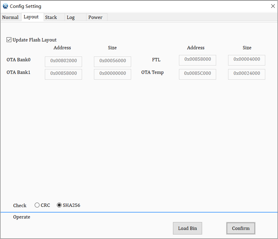
Generate Config File through MP Tool
For the convenience of users, Realtek provides Flash Map Generate Tool for Flash layout files. The explanation is as follows:
flash map.inifile -- can be imported into MP Tool to generate Config File and OTA header.flash_map.hfile -- needs to be copied to the APP project directory to compile a correct and runnable APP image.

Flash Map Generate Tool Configures Flash Map
But at the same time, the following principles must be followed to adjust the flash layout.
If choosing the supporting Bank switching scheme, ensure that the size of OTA Bank0 is equal to the size of OTA Bank1, and set the size of the OTA TMP area to 0.
If choosing the non-supporting Bank switching scheme, set the size of OTA Bank1 to 0, and the size of the OTA TMP area should not be smaller than the size of the largest image in OTA Bank0.
In order to lock all the code areas to prevent unexpected flash write and erase operations, align the offset of the end address of OTA Bank1 relative to the start address of the flash to the actually selected flash address as much as possible. Please refer to Software Block Protect.
Flash Layout Example
Based on the Flash Layout Adjustment, this section provides examples of the flash layout under Supporting Bank Switching Scheme and Non-supporting Bank Switching Scheme.
Supporting Bank Switching Scheme
Sample Layout for Flash (total size = 1MB) |
Size(Bytes) |
Start Address |
|---|---|---|
Reserved |
4K |
0x00800000 |
OEM Header |
4K |
0x00801000 |
OTA Bank0 |
344K |
0x00802000 |
|
4K |
0x00802000 |
|
4K |
0x0080A000 |
|
28K |
0x00803000 |
|
28K |
0x0080B000 |
|
144K |
0x00812000 |
|
132K |
0x00836000 |
|
0K |
0x00857000 |
|
0K |
0x00857000 |
|
0K |
0x00857000 |
|
0K |
0x00857000 |
|
0K |
0x00857000 |
|
4K |
0x00857000 |
OTA Bank1 |
344K |
0x00858000 |
|
4K |
0x00858000 |
|
4K |
0x00860000 |
|
28K |
0x00859000 |
|
28K |
0x00861000 |
|
144K |
0x00868000 |
|
132K |
0x0088C000 |
|
0K |
0x008AD000 |
|
0K |
0x008AD000 |
|
0K |
0x008AD000 |
|
0K |
0x008AD000 |
|
0K |
0x008AD000 |
|
4K |
0x008AD000 |
FTL |
16K |
0x008AE000 |
OTA TMP |
0K |
0x008B2000 |
user data1 |
0K |
0x008B2000 |
user data2 |
0K |
0x008B2000 |
Note
Flash Layout should be determined based on the actual size of the image and data.
Non-supporting Bank Switching Scheme
Sample Layout for Flash (total size = 512KB) |
Size(Bytes) |
Start Address |
|---|---|---|
Reserved |
4K |
0x00800000 |
OEM Header |
4K |
0x00801000 |
OTA Bank0 |
344K |
0x00802000 |
|
4K |
0x00802000 |
|
4K |
0x0080A000 |
|
28K |
0x00803000 |
|
28K |
0x0080B000 |
|
144K |
0x00812000 |
|
132K |
0x00836000 |
|
0K |
0x00857000 |
|
0K |
0x00857000 |
|
0K |
0x00857000 |
|
0K |
0x00857000 |
|
0K |
0x00857000 |
|
4K |
0x00857000 |
OTA Bank1(Equal to 0) |
0K |
0x00858000 |
FTL |
16K |
0x00858000 |
OTA TMP |
144K |
0x0085C000 |
user data1 |
0K |
0x00880000 |
user data2 |
0K |
0x00880000 |
Note
The space for APP data is not allocated in this sample. Flash Layout should be distributed based on the actual size of image and data.
Image Format
All images that support upgrades in OTA Bank Flash Segmentation are composed of a 1024-byte image header and a variable-length payload.
The image header contains the image type, size, version number, hash value, signature information, etc. The definitions of each field in the image header are as follows:
Memory Segment |
Size(Bytes) |
Functions |
|---|---|---|
image_cmac |
16 |
CMAC value of the image, used for authentication when secure boot is enabled. |
image_signature |
384 |
Signature of the image, used for authentication when secure boot is enabled. |
image_hash |
32 |
Hash check for the image, used for verifying the integrity of the image. |
image_control_header |
12 |
Control information of the image, for details please refer to image_control_header format. |
uuid |
16 |
UUID value of the image. |
exe_base |
4 |
Execution address of the image. |
load_src |
4 |
Starting address of the code loaded into RAM. |
load_len |
4 |
Size of the code loaded into RAM |
image_base |
4 |
Flash address of the image. |
dev_id |
2 |
Not used. |
flash_layout_size_4k, |
2 |
Size of the flash layout. (unit: 4KB) |
magic_pattern |
4 |
Pattern information of the image. |
dec_key |
16 |
Not used. |
load_dst |
4 |
Starting address of the code loaded into Flash. |
ex_info |
24 |
Information of the heap and the RAM. |
git_ver |
16 |
Version information of the image. |
RSA Public Key |
388 |
Used for authentication when secure boot is enabled. |
image_info |
92 |
For the OTA Header, image_info represents the starting address and size of each image in the OTA Bank. For other images, image_info is reserved. |
image_control_header format in image header is shown as follows:
  typedef struct _IMG_CTRL_HEADER_FORMAT
  {
      uint16_t crc16;
      uint8_t ic_type;
      uint8_t secure_version;
      union
      {
          uint16_t value;
          struct
          {
              uint16_t xip: 1; // payload is executed on flash
              uint16_t enc: 1; // all the payload is encrypted
              uint16_t load_when_boot: 1; // load image when boot
              uint16_t enc_load: 1; // encrypt load part or not
              uint16_t enc_key_select: 3; // referenced to ENC_KEY_SELECT
              uint16_t not_ready: 1; // for copy image in ota
              uint16_t not_obsolete: 1; // for copy image in ota
              uint16_t integrity_check_en_in_boot: 1; // enable image integrity check in boot flow
              uint16_t compressed_not_ready: 1;
              uint16_t compressed_not_obsolete: 1;
              uint16_t rsvd: 1;
              uint16_t image_type: 3; /* for app 000b: normal image, 001b: compressed image, other for more types
              for patch in temp bank consist of 001b: patch+fsbl, 010b: patch+app, 011b: patch+fsbl+app*/
          };
      } ctrl_flag;
      uint16_t image_id;
      uint32_t payload_len;
  } T_IMG_CTRL_HEADER_FORMAT;
Parameter description:
- ic_type:
indicates IC type, the value for RTL8752H IC type is 16.
- secure_version:
indicates the version of the boot security check image.
- image_id:
identifies different types of image, among which SCCD, OCCD cannot be updated through DFU.
typedef enum
{
    IMAGE_FIRST = 0x278D,
    SCCD        = 0x278D,
    OCCD        = 0x278E,
    FactoryCode = 0x278F,
    OTA         = 0x2790, /**< OTA header */
    SecureBoot  = 0x2791,
    RomPatch    = 0x2792,
    AppPatch    = 0x2793,
    AppData1    = 0x2794,
    AppData2    = 0x2795,
    AppData3    = 0x2796,
    AppData4    = 0x2797,
    AppData5    = 0x2798,
    AppConfigFile = 0x2799,
    UpperStack  = 0x279a,
    IMG_BT_STACKPATCH = 0x279b,
    IMAGE_MAX,

    IMAGE_USER_DATA2 = 0xFFFD,  /**< the image only supports unsafe single bank ota*/
    IMAGE_USER_DATA = 0xFFFE,  /**< the image only supports unsafe single bank ota*/
} T_IMG_ID;
Parameter description:
- payload_len:
indicates the size of the image, not including the 1024 bytes of the image header. The total length of the image is the payload_len plus 1024 bytes.
- crc16:
indicates the crc16 checksum of the image. By default, the image uses SHA256 for verification, and the checksum is stored in image_hash. The crc16 can be ignored.
- ctrl_flag:
the only bit fields related to DFU are not_ready and not_obsolete.
not_ready: indicates whether the image is valid. By default, the not_ready field in the image header of files published, compiled, or generated by tools is all 0.
There is a risk of power outage when transferring the image to the backup area via Bluetooth. Therefore, before writing to the backup area, it is necessary to change not_ready to 1 and then write to the flash.
Only when the image transfer is complete and the image integrity check is successful, modify the not_ready in the backup area image to 0, indicating the backup area image is valid.
After the system restarts, the activation process of the backup image is completed by the BootLoader.
not_obsolete: indicates if the image should be abandoned and its default value is 1.
When bank switching is supported, not_obsolete is invalid during the DFU process.
When bank switching is not supported, after the DFU upgrade is complete, the boot code determines that not_ready is 0 and not_obsolete is 1. At this time, the image will be transferred from the OTA TMP area to the corresponding image run area in OTA Bank0. After the transfer is successful, write the not_obsolete in the OTA TMP area image to 0 to prevent repeated transfers. This ensures that the upgraded image is properly installed and run, and the old image is marked as obsolete to avoid being used again.