Platform Overview
In this chapter, we will introduce the RTL8752H platform from an overall perspective, including Hardware Architecture, Software System, and how to use the SDK for Application Development. Additionally, this chapter also covers important topics such as the Boot Flow, Interrupt Management, and the Principle of BLE Applications to help developers fully grasp platform resources and achieve efficient development.
If developers want to quickly get started with the RTL8752H evaluation board and run their first application, they can visit Quick Start.
Hardware Architecture
The CPU of the RTL8752H is Cortex-M0+ (based on ARMv6-M architecture), with a maximum frequency of 40MHz.
RTL8752H Hardware Architecture mainly consists of the following hardware units:
Rich peripherals
Power management unit
Clock management unit
RF module

RTL8752H Hardware Architecture
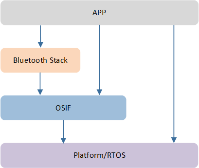
Software System
Software Architecture
RTL8752H Software Architecture mainly consists of the following levels:
Platform Features: Includes Flash Driver, Clock Manager, Power Manager, OTA, etc.
Peripheral Driver: Provides interfaces for application layer to access RTL8752H peripherals.
Bluetooth LE Stack: Realtek's implementation of BT Controller and BT Host.
GAP: An abstraction layer for interaction between application and BLE protocol stack.
OSIF: An abstraction layer of RTOS (Real-Time Operating System) provided by Realtek.

RTL8752H Software Architecture
Operating System
RTL8752H supports multiple RTOS, with FreeRTOS V10.4.4 as the default.
Note
FreeRTOS on RTL8752H runs on ROM.
OSIF
OS Interface (OSIF) is an OS interface layer abstracted by Realtek. OSIF provides a unified interface by encapsulating specific RTOS interfaces.
The greatest advantage of using OSIF is: if developers want to run upper layer applications on different RTOS, they can port the specific RTOS interfaces to the OSIF without needing to make any modifications to the upper layer software. Therefore, we highly recommend developers to use the OSIF interface when developing applications rather than directly accessing specific RTOS interfaces.
OSIF Architecture
Note
For OSIF header files, please refer to inc/os/os_*.h.
Tasks
The design of RTL8752H Task is based on FreeRTOS, and by default supports preemptive threads. Its task priority can be set from 0 to 6, with higher numbers indicating higher priority.
The tasks created by the system include:
FreeRTOS will by default create a Timer task and an Idle task.
The Bluetooth protocol stack will by default create a Bluetooth Controller task and a Bluetooth Host task.
In FreeRTOS, tasks by default support preemption. Applications can create tasks according to actual needs, with priority recommended to be set between 1 and 4.
Task |
Description |
Priority |
|---|---|---|
Timer |
Task for implementing software timers using FreeRTOS |
6 |
Bluetooth Controller |
Implementation of protocol stack below the Bluetooth HCI layer |
6 |
Bluetooth Host |
Implementation of protocol stack above the Bluetooth HCI layer |
5 |
APP |
Implementation of application layer functions |
suggested priority is 1~4 |
Idle |
Background idle tasks including low-power processing |
0 |
Boot Flow
The RTL8752H system, upon power-up or restart, will execute the boot flow, as described below:
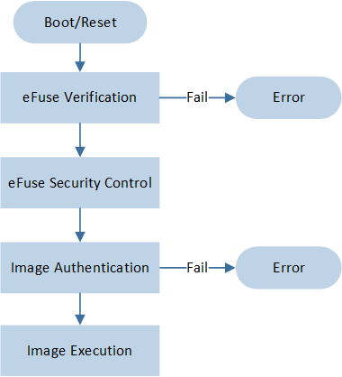
Boot Flow
Action |
Description |
|---|---|
eFuse Verification |
Verify the values in eFuse; if verification fails, the system boot fails. |
Security Control |
Perform corresponding security controls based on eFuse settings, such as whether SWD is open, updating Boot Config settings, etc. |
|
|
Image Execution |
After the image authentication, execute the specified image sequentially according to the designed process. |
Image Authentication
The Image Authentication flow in the RTL8752H startup is shown in the following figure:
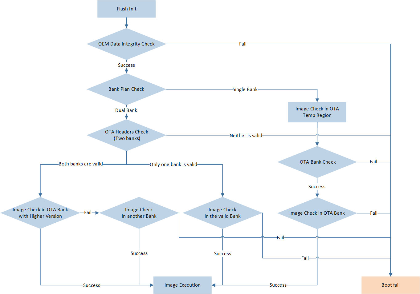
Image Authentication Flow
Note
OEM Data is also known as the Config File, which contains important parameters set for the RTL8752H, such as the layout information of the images.
OTA Strategy
The OTA strategy for RTL8752H supports both single bank and dual bank schemes. The boot code will determine the OTA strategy based on the image layout in the OEM Data:
Check whether a valid pending upgrade image exists in the Temp area. If it exists, verify it. If verification passes, move it to the corresponding position in the bank.
Verify the OTA bank header.
Verify the images in the OTA bank in sequence.
Execute the specified images.
-
Verify the two OTA bank headers. Based on the verification results, there are the following three scenarios:
Scenario One: Both OTA bank headers pass verification. Then, in the subsequent process, the OTA bank with the updated version is used, and the other OTA bank serves as a backup.
Scenario Two: Only one OTA bank header passes verification. Then, the subsequent process uses that OTA bank.
Scenario Three: Both OTA bank headers fail verification, resulting in a boot failure.
Verify the images in the OTA bank in sequence. If it is Scenario One and a certain image fails verification, the system will switch to the backup OTA bank and verify the images in that backup bank.
Execute the specified images.
Note
Please refer to the OTA User Guide for OTA information.
Please refer to Image Layout for more information on 'Image Layout'.
Authentication Method
Depending on whether the Secure Boot function (determined by eFuse) is enabled, the image authentication method can be divided into:
Supports using SHA256 and CRC16 for integrity checks.
During the authentication process, if an image fails the check, the system will continue with the subsequent Image Execution process but will issue an Error Log to alert the developer.
Supports using RSA and CMAC for signature verification.
During the authentication process, if an image fails the check, the system will halt the execution of subsequent processes and perform Error handling.
Image Decryption
After an image is successfully authenticated, it will additionally check whether the image is encrypted. If the image is encrypted, the information of encryption area and key will be registered into the Flash On-The-Fly engine. For details, please refer to: Security Mechanism.
Memory
The memory system of RTL8752H includes ROM, RAM, Flash, and eFuse. For details, please refer to Memory.
Flash Driver and FTL related content, please refer to Flash.
Interrupt Management
The interrupt management of RTL8752H is based on the NVIC (Nested Vectored Interrupt Controller) system of Cortex-M. The interrupt parameters of RTL8752H are as follows:
16 Cortex-M0+ system exceptions
32 maskable interrupt channels (including two interrupts with second-level sub-interrupts)
4 programmable interrupt priorities
The NVIC closely integrates with the processor core interface, making low-latency interrupt handling and efficient delay interrupt processing possible.
Interrupt Vector Table
The interrupt vector table is used to manage and handle different types of interrupts. It is a data structure stored in memory, containing the entry addresses of the ISR (Interrupt Service Routine). The system can quickly locate and invoke the ISR related to the interrupt types via interrupt vector table, thereby improving the system's response speed and efficiency.
RTL8752H's interrupt vector table is placed on a certain region in RAM. Developers can update the specified ISR in the interrupt vector table through the API RamVectorTableUpdate().
Exception Number |
CMSIS-CORE enumeration value |
Exception Type |
Description |
|---|---|---|---|
1 |
Reset |
Reset |
|
2 |
[-14] |
NMI |
Non-Maskable Interrupt. The Watchdog is linked to the NMI vector |
3 |
[-13] |
HardFault |
Fault handling exception |
4 ~ 10 |
Reserved |
||
11 |
[-5] |
SVCall |
Supervisor call via SVC instruction |
12~13 |
Reserved |
||
14 |
[-2] |
PendSV |
Pendable request for system service |
15 |
[-1] |
SysTick |
System Tick Timer |
16 |
[0] |
System Interrupt |
Interrupt the CPU when the system is awakened by a GPIO event. |
17 |
[1] |
Internal use |
Internal use |
18 |
[2] |
BT MAC |
BT MAC Interrupt |
19 |
[3] |
Timer3 |
Timer3 Global Interrupt |
20 |
[4] |
Timer2 |
Timer2 Global Interrupt |
21 |
[5] |
Internal use |
Internal use |
22 |
[6] |
I2S0_TX |
I2S0 TX Interrupt |
23 |
[7] |
I2S0_RX |
I2S0 RX Interrupt |
24 |
[8] |
Timer4_5 |
Timer4~5 interrupt has secondary interrupts. Refer to Timer4~5 Interrupt. |
25 |
[9] |
ZIGBEE |
ZIGBEE Interrupt |
26 |
[10] |
PF_RTC |
Platform RTC Interrupt |
27 |
[11] |
RTK_UART0 |
RTK UART0 Interrupt |
28 |
[12] |
RTK_UART1 |
RTK UART1 Interrupt |
29 |
[13] |
I8080 |
I8080 Interrupt |
30 |
[14] |
SPI0 |
SPI 0 Interrupt |
31 |
[15] |
SPI1 |
SPI 1 Interrupt |
32 |
[16] |
I2C0 |
I2C 0 Interrupt |
33 |
[17] |
I2C1 |
I2C 1 Interrupt |
34 |
[18] |
ADC |
ADC Global Interrupt |
35 |
[19] |
Peripheral |
Peripheral interrupt has secondary interrupts. Refer to Peripheral Interrupt. |
36 |
[20] |
DMA_Channel0 |
RTK-DMA channel0 Global Interrupt |
37 |
[21] |
DMA_Channel1 |
RTK-DMA channel1 Global Interrupt |
38 |
[22] |
DMA_Channel2 |
RTK-DMA channel2 Global Interrupt |
39 |
[23] |
DMA_Channel3 |
RTK-DMA channel3 Global Interrupt |
40 |
[24] |
Enhanced_Timer0 |
Enhanced Timer 0 Interrupt |
41 |
[25] |
Enhanced_Timer1 |
Enhanced Timer 1 Interrupt |
42 |
[26] |
GPIO_Group3 |
|
43 |
[27] |
GPIO_Group2 |
|
44 |
[28] |
IR |
IR module global Interrupt |
45 |
[29] |
GPIO_Group1 |
|
46 |
[30] |
GPIO_Group0 |
|
47 |
[31] |
RTK_UART2 |
RTK UART 2 Interrupt |
Exception Number |
Exception Type |
Description |
|---|---|---|
48 |
Timer4 |
Timer4 Interrupt |
49 |
Timer5 |
Timer5 Interrupt |
Exception Number |
Exception Type |
Description |
|---|---|---|
50 |
SPIC0 |
SPIC0 Flash Interrupt |
51 |
Qdecode |
Qdecode Global Interrupt |
52 |
Keyscan |
Keyscan Global Interrupt |
53 |
SPI2W |
2-wire/3-wire SPI Interrupt |
54 |
LPCOMP |
Analog Comparator Interrupt |
55 |
PTA_Mailbox |
MailBox Interrupt |
56 |
SPIC1 |
SPIC1 Flash Interrupt |
57 |
SHA256 |
SHA256 Interrupt |
58 |
Platform |
Platform Interrupt |
59 |
TRNG |
TRNG Interrupt |
61 |
FLASH_SEC |
Flash On-The-Fly Interrupt |
62 |
RTC |
Real Time Counter Interrupt |
63 |
WDT |
Watchdog Global Interrupt |
GPIO Group 3 Interrupt |
GPIO Group 2 Interrupt |
GPIO Group 1 Interrupt |
GPIO Group 0 Interrupt |
|---|---|---|---|
GPIO3 |
GPIO2 |
GPIO1 |
GPIO0 |
GPIO7 |
GPIO6 |
GPIO5 |
GPIO4 |
GPIO11 |
GPIO10 |
GPIO9 |
GPIO8 |
GPIO15 |
GPIO14 |
GPIO13 |
GPIO12 |
GPIO19 |
GPIO18 |
GPIO17 |
GPIO16 |
GPIO23 |
GPIO22 |
GPIO21 |
GPIO20 |
GPIO27 |
GPIO26 |
GPIO25 |
GPIO24 |
GPIO31 |
GPIO30 |
GPIO29 |
GPIO28 |
Interrupt Priority
RTL8752H supports four programmable interrupt priorities. However, to maintain compatibility with other SoCs in the Realtek Bee series (most support 8 priority levels),
the Irq-Priority-Bits-Number of RTL8752H is set to 3, resulting in the following interrupt priority relationship: (0 = 1) > (2 = 3) > (4 = 5) > (6 = 7) .
It is recommended to follow the rule in the table below when setting interrupt priority:
Priority |
Rule |
|---|---|
0/1 |
Used for interrupts with very high real-time requirements. BT MAC Interrupt uses this priority level by default. |
|
2/3 4/5 |
Generally used for ordinary peripheral interrupts. |
6/7 |
SysTick and PendSV. |
Note
The ARMv6-M architecture used by RTL8752H does not support dynamic adjustment of interrupt priorities. If adjustment of interrupt priorities is needed, the interrupt must be disabled first, modify the interrupt priority, and then re-enable the interrupt.
Power Mode
RTL8752H supports the following four power modes:
Power Mode |
Description |
|---|---|
CPU Active |
The system is in a fully powered and active state. |
CPU Sleep |
The system enters the WFI state. In this mode, the CPU clock will automatically slow down. |
The system enters a lower power consumption state. The system enters a sleep mode with quicker entry and exit times, while maintaining the contents of the RAM. |
|
Power Down |
The system enters an extremely low power consumption state. In this mode, RAM contents are not retained. Exiting from Power Down mode will initiate a restart process, which takes longer than exiting from DLPS mode. |
RTL8752H will enter a specific power state when certain conditions are met and wake up the system under specific conditions. For more details, please refer to Low Power Mode.
Application Development
SDK Architecture
Before developing applications, please familiarize yourself with the SDK of RTL8752H. Its directory structure is as follows:
└── SDK
    ├── bin                   Used to store compiled executable files or binary files.
    ├── board                 Contains some sample projects, allowing developers to understand how to develop applications on this evaluation board.
        ├── evb
            └── samples
    ├── doc                   Stores SDK-related documentation.
    ├── inc                   Contains various header files, divided into the following subdirectories:
        ├── app               Header files related to applications, defining application-level interfaces.
        ├── bluetooth         Header files related to Bluetooth functionality, including Bluetooth protocol stack, configuration, etc.
        ├── os                Header files related to the operating system, including interface definitions for OSIF and FreeRTOS.
        ├── peripheral        Header files related to peripherals, such as GPIO, UART, SPI, I2C, etc.
        └── platform          Header files related to the platform, defining platform-level interfaces and configurations.
    ├── src                   Contains source files (.c, .s, etc.) that implement specific functions.
    └── tools                 Contains tools and scripts for compiling, programming, and debugging.
Sample Project
To help developers quickly get started with application development, many sample projects have already been created in the RTL8752H SDK. For detailed introductions and references to the sample projects, please refer to Samples.
Note
Since sample projects may be updated along with the SDK, it is recommended to organize the newly added code in a module to better utilize the latest example code.
Project Organization
Taking the Keil project of ble_peripheral as an example, it is organized into the following modules for source files:
Project Directory |
Description |
|---|---|
Include |
Contains ROM UUID files. |
CMSIS |
Contains startup code. |
Lib |
Contains all binary files used by the application. |
Peripheral |
Contains all peripheral drivers and module code used by the application. |
Profile |
Contains BLE profiles or services used by the application. |
APP |
Implementation of ble peripheral application. |
Common Files
Each sample project in the RTL8752H SDK includes the following common files:
File Name |
Description |
|---|---|
|
UUID header file used by the application to identify ROM, no modification needed. |
|
ROM symbol library, links symbols in the ROM for the application. |
|
links symbols in the ROM for the lower stack. |
|
Realtek extension function library. |
|
GAP library implementing BLE functions |
|
Assembly file for the startup of RTL8752H applications. |
|
C file for the startup of RTL8752H applications. |
|
Header file for configuration scripts and low power mode. |
|
Flash layout file, generated by Flashmap Generate Tool. |
|
File related to memory configuration. |
Principle of BLE Applications
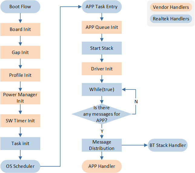
The execution flow of BLE applications provided in the RTL8752H SDK is as follows:
Execution Flow of BLE Applications
Initialization
BLE applications start initialization within the main() function, and the explanation of initialization actions realized by realtek is as follows:
Action |
Description |
|---|---|
Board Init |
Initialization settings for PINMUX and PAD |
Gap Init |
Initialization of GAP-related parameters |
Profile Init |
Initialization of BLE Profiles |
Power Manager Init |
Initialization related to power management |
SW Timer Init |
Initialization of software timers |
APP Queue Init |
Initialization of APP Queue including io msg queue and event queue |
Driver Init |
Initialization of peripherals |
Message and Event Handling Mechanism
In BLE applications, both the Bluetooth protocol stack and peripherals interact with the APP layer through the Message and Event Handling Mechanism.
The essence of the message and event handling mechanism is that messages (IO MSG) are encapsulated into events (Event), and these events are then distributed and processed in the message handler at the APP layer.
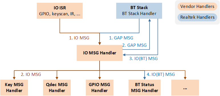
Message and Event Handling Mechanism
As shown in the above figure, after the original message is encapsulated into an Event, it will be sent to the corresponding queue. Upon receiving the Event, the message dispatcher at the APP layer calls the corresponding MSG Handler to process it based on the Event type:
If the Event type is IO MSG: it is forwarded by the message dispatcher to a specific IO MSG Handler for processing.
If the Event type is MSG from the Bluetooth protocol stack: it is first forwarded by the message dispatcher to the BT state machine. After the BT state machine processes the MSG, it is then encapsulated into a BT IO MSG and sent to the queue.
Developers are responsible for the following when developing applications:
Implement the ISR for the peripheral, completing preliminary processing within the ISR. If further processing is needed, encapsulate the Event and send it to the APP.
Expand the message dispatcher as needed to receive and process user-defined MSGs.
Implement the MSG Handler related to the application layer.
Expand the custom Message Type and Subtype as required.
Note
The specific implementation of this section can be found in the sample project files:
app_task.candapp_flag.h.The GAP layer notifies the APP layer through a message and event handling mechanism, while the APP layer can directly call the GAP layer's APIs to notify the GAP layer.
Pin Settings
The definitions of the pins are defined in board.h.
#define KEY_0   P4_0
#define BEEP    P4_1
#define LED_0   P2_1
#define LED_1   P2_4
Power Mode Settings
In the sample project, developers can control whether to enable the low power mode through Realtek's predefined macros:
For most of the projects: the macro
DLPS_ENinboard.his used to control whether to enter low power consumption mode.For BLE-related projects: the macro
F_BT_DLPS_ENinapp_flags.his used to control whether to enter low power consumption mode.
For details, please refer to Low Power Mode.
Debugging
The application program can be debugged in the following two ways:
Use the log mechanism to trace the execution of the code and data.
Use Keil MDK or J-Link Commander and SWD for debugging, add/remove breakpoints, and access/trace memory, etc.
For details, please refer to Debug System.
See Also
Please refer to the relevant API Reference: