Flash, as a type of non-volatile memory, differs from RAM. RAM allows direct reading and writing, direct code execution and data storage. However, flash writing operations can only be performed in empty or already erased cells. Therefore, an erase operation must be performed before executing a flash write operation.
Note
Flash has a programming limit up to 100,000 cycles. Frequent erasing and writing at a specific block can easily lead to bad blocks.
When users need to use flash to store data, the flash driver interface is not primarily recommended for APP. It is more advisable to use the FTL interface.
The RTL8752H integrates a Flexible Memory Controller (FMC), supporting external SPI flash. The FMC supports a maximum address mapping space of 16M bytes, corresponding to the address space 0x00800000~0x017FFFFF. The specific usable space of the flash is determined by flash model. For more detailes, please refer to: Flash Layout.
FTL (Flash Translation Layer) is a software abstraction layer implemented based on flash drivers, used for users to read and write flash data. The physical location of FTL can be viewed at Flash Layout. The purpose of FTL is to simplify the process of modifying flash data.
If FTL is not used, when flash data need to be modified, flash erase operation must be called first. Frequent flash data modifications result in a significant amount of time wasted on erasing. However, FTL uses logical addresses instead of physical addresses to access flash. When users modify data, the original data is not directly altered. Instead, the new data is written to a new physical address, and the logical address points to this physical address. This method can avoid frequent flash erase, saving the time required for data modification.
When FTL detects that there isn't enough space to write a new record, Garbage Collection (GC) mechanism is triggered to erase and reclaim expired or unused records. FTL, by cyclically using flash space and evenly distributing write and erase operations, can prevent certain blocks from becoming invalid before reaching P/E cycles, therefore achieving wear leveling.
Note
FTL is suitable for data that requires frequent rewriting. On one hand, the API interface is simpler, and on the other hand, it helps to extend the lifespan of the flash (wear leveling).
If the data volume is large, read-only (or occasionally rewritten), and does not need to support OTA upgrades, it is recommended to use the flash API to store data in the 'APP Defined Section' area.
If the data volume is large, read-only (or occasionally rewritten), and needs to support OTA upgrades, it is recommended to store data in the App Data1, App Data2, App Data3, App Data4, and App Data5 areas within the OTA bank.
The logical address starts at 0x0400, and the end address is related to otp configuration, with the default FTL_REAL_LOGIC_ADDR_SIZE being 3KB.
It is used to store APP information.
The following APIs can be used to read/write APP storage data: ftl_save() and ftl_load().
Note
In the implementation of the ftl_save() API and ftl_load() API, the offset parameter passed in has already been added with the offset 0x0400 of the APP storage space, so when the APP uses these two APIs, the offset parameter can start from 0.
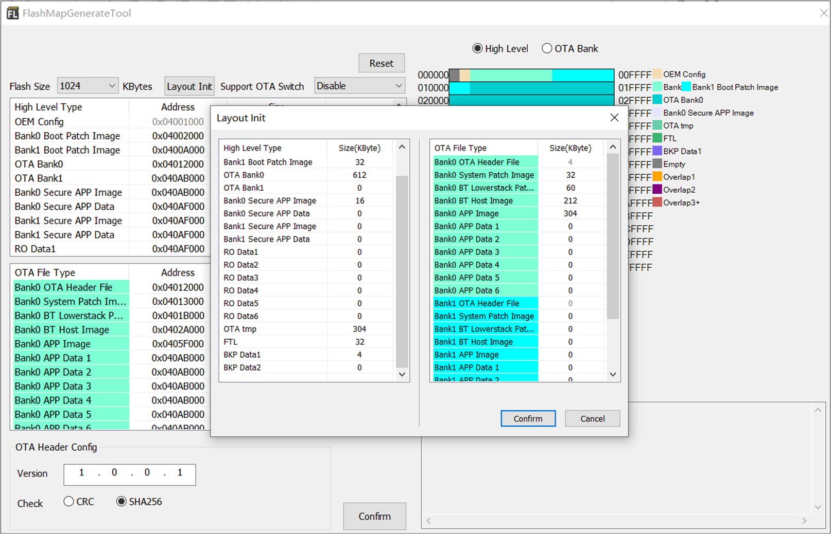
The physical size of FTL is configurable by modifying the configuration parameters in the config file. The steps are as follows:
Use the Flash Map Generate Tool (released with the MP Tool) to generate flash_map.ini and flash_map.h files.
Copy the flash_map.h file to the APP project directory, for example: sdk\samples\bluetooth\ble_peripheral, so that the APP can obtain the correct loading address during compilation.
Load the flash_map.ini generated in the first step into the MP Tool to generate a config file for download, as shown in the example Modify Flash Map Configuration File, adjusting FTL physical space to 32K.
When adjusting the physical size of FTL, the maximum logical space available to the APP will also change accordingly. Assuming the actual physical size of FTL is set to mKB (where m is a multiple of 4), the maximum logical space available to the APP equals \(((511*(m-4) - 4) - 3328)\) bytes.
To enhance the efficiency of FTL reading, a mapping mechanism between physical and logical addresses is implemented at the lower level, which occupies some RAM space. With the default FTL physical size set to 16KB, this mapping table occupies 2298 bytes of RAM HEAP space. Assuming the actual FTL physical size is set to mKB (where m is a multiple of 4), the mapping table occupies \(((511 * (m-4) - 4) * 0.375)\) bytes of RAM space.
When adjusting FTL space size, users need to adjust reasonably based on the specific application scenario. If set too large, it will waste some RAM resources. On the other hand, if a relatively small flash is chosen and you want to compress the space occupied by FTL, you must ensure that FTL physical space is not less than 12KB. Since each logical address in the mapping table corresponds to a physical address using 12-bit by default, FTL physical space can be adjusted up to a maximum of 32KB.
In addition to the standard Serial Peripheral Interface (SPI), most flash memories also support high-performance dual/quad-bit mode I/O SPI, controlled by the following six pins.
The standard SPI mode, also known as 1-bit mode, uses only CLK, CS#, DI, and DO. WP# serves as the write-protect input, while HOLD# serves as the hold function input.
Dual Bit Mode
Uses CLK, CS#, and uses DI, DO as IO0, IO1 respectively. The functions of WP# and HOLD# remain the same as in single bit mode.
Quad Bit Mode
Uses CLK, CS#, and uses DI, DO, WP#, HOLD# as IO0, IO1, IO2, IO3 respectively. As all six pins are used, write protection and hold functions are unavailable in quad-bit mode.
Note
Currently, the flash used by RTL8752H only partially supports quad-read mode. Users should verify the flash model and characteristics in advance.
To support more flash models, RTL8752H defaults to 1-bit mode at startup. If users wish to switch to a high-speed bit mode (2 or 4-bit mode), they can call the interface provided in the SDK: flash_nor_try_high_speed_mode to switch to high-speed bit mode. The 'mode' parameter configures the flash to attempt switching to the desired high bit mode. If the switch fails, it will revert to 1-bit mode.
The prototype of the interface function provided in the SDK for bit mode switching is as follows.
Flash has multiple protection mechanisms to prevent accidental erase or writing. The two main protection mechanisms are software block protection and hardware pin protection.
Locking the flash via the hardware protection pin (#WP) has the following two drawbacks:
If the #WP pin is used as a protection function, the flash's quad mode cannot be used.
Hardware protection can only choose to protect the entire flash or not protect it at all. It cannot protect a portion of flash.
The RTL8752H uses a more flexible mechanism, Software Block Protect (BP), to prevent accidental flash erase and writing operations. The principle is to use some BP bits in the flash status register to select the range to be protected. By default, the RTL8752H uses the BP function to protect some important data (such as configured parameters) and code segments, rather than the entire flash space. Flash uses the BP (X) bits in the status register to identify the number of blocks to be locked, and the TB bit to determine the locking direction. The RTL8752H only supports locking starting from the low address end of the flash.
Software block protection levels varies depending on the flash model used. The main models currently in use and their protection levels are as follows:
Regular software block protection levels, such as GD25WD80, GD25WD40, ZB25WD80B, and ZB25WD40B.
Irregular software block protection levels, such as P25Q40SU and P25Q80SU.
Below, the software block protection levels of GD25WD80 and P25Q40SU are used as examples to illustrate these two flash locking level pattern.
The software block protection levels of GD25WD80 are shown in the figure below. It supports full lock, no lock and the minimum lock region is 768KB. For this catogory, if locking to 1/2 is possible, RTL8752H supports full lock, no lock, and lock 1/2 these three locking options. Other levels are not supported. If locking to 1/2 is not possible, only full lock and no lock are supported.
The software block protection levels of P25Q40SU are shown in the figure below. Starting from full lock, it can lock 1/2, 1/4, 1/8 until no lock at all. For this regular catogory, all software block protection levels provided by the flash can be set.
For user convenience, RTL8752H offers an automatic locking mechanism controlled by macro DEFAULT_FLASH_BP_LEVEL_ENABLE. When #defineDEFAULT_FLASH_BP_LEVEL_ENABLE1 is defined in header file otp_config.h, RTL8752H will lock to the maximum possible range based on the configured flash layout and the selected flash model, which is from the flash start address to the OTA bank1 end address (refer to flash layout: Flash Layout). Most flash support flash protection by level, such as different sizes of regions like 64KB, 128KB, 256KB, 512KB, etc.
When dividing the flash layout, try to align the OTA bank1 end address offset with a range supported by the flash protection level. This aims to fully lock important data and code areas without affecting the subsequent area that needs to be rewritten, such as the 'FTL', 'OTA Tmp' area. Once the flash layout is determined, RTL8752H will automatically parse the flash layout configuration parameters and query the selected flash information to set the BP protection level. When the used flash model only supports block protection as shown in GD25WD80 Software Block Protection, RTL8752H will choose not to lock.
In summary, RTL8752H supports two locking methods:
This method is more direct and unrestricted, but the bp_lv needs to be calculated by users according to the corresponding flash datasheet.
Enable macro DEFAULT_FLASH_BP_LEVEL_ENABLE to use the automatic locking mechanism.
With this method, users do not need to calculate bp_lv, but it will fail to lock when the used flash model only supports block protection as shown in GD25WD80 Software Block Protection.
Note
As the current version of OTA demo does not yet support upgrades when the flash is locked, it is currently not recommended to use this feature.
The power consumption modes of flash are mainly divided into the following three scenarios.
Working mode: Power consumption is generally in the 10 mA range.
Standby mode: Power consumption is generally around tens of uA.
Power Down mode: Power consumption is even lower, sometimes less than 1 uA.
The details are as follows:
Flash automatically enters standby mode when not accessed and will automatically enter working state when access is needed.
To enter Power Down mode, a specific command is required:
Most flash use command 0xB9 to enter Power Down mode
Command 0xAB to exit Power Down mode.(While MXIC by toggling the #CS pin)
Note
It should be noted that after the flash enters Power Down mode, receiving any command other than the exit Power Down command (0xAB) is dangerous. This is because, after entering Power Down mode, the flash only accepts wake-up commands to exit Power Down mode, all other commands will be ignored, but the flash controller may enter an infinite loop waiting for the flash's response.
To prevent the risks associated with the misuse of Flash Power Down mode, the system's DLPS mechanism has incorporated control of the Flash Power Down mode: when entering DLPS, an instruction is automatically issued to put the flash into Power Down mode, and upon exiting DLPS, the flash is awakened.
XIP refers to allowing code to execute directly from flash without having to be copied to RAM. This saves RAM space, and if there is enough remaining RAM space, the APP code can execute directly on RAM, which helps improve performance and reduce power consumption. If the remaining RAM space is insufficient, part or all of the APP code needs to be executed on flash. The relevant configurations for executing XIP on RTL8752H are summarized as follows.
Macro FEATURE_RAM_CODE
Configured in mem_config.h:
When set to 1, code without any section modifiers by default will execute on RAM.
When set to 0, code without any section modifiers by default will execute in flash.
Section Decoration
Reference app_section.h
APP_FLASH_TEXT_SECTION: Specifies that the code section is executed on flash.
APP_RAM_TEXT_SECTION: Specifies that the code section is executed on RAM.
Note
If there is insufficient RAM space, prioritize executing time-sensitive code on RAM to ensure efficiency.
Ways to Improve the Efficiency of Executing XIP Code
The RTL8752H, with support from FMC, can use automatic mode to read flash and directly execute code on the SPI flash. However, users might perform read, write, and erase operations on the flash in user mode by calling the provided interface. The flash access operations in user mode are not atomic; if interrupted by another automatic mode access operation, it may lead to flash access anomalies. To ensure the atomicity of flash access operations in user mode, the following usage restrictions and precautions must be observed during XIP.
Note
The interfaces provided for user mode access to flash in RTL8752H have a '_locked' suffix, and by default, critical section protection is added, which will disable all interrupts. If the flash operation takes too long, such as writing a large amount of data at once, it is recommended to split the writing action into multiple smaller data write actions to avoid missing interrupts due to excessively long interrupt disable times.