IO
This document is intended to help beginners quickly become familiar with the peripherals of RTK MCU. It introduces various peripherals, including PINMUX, PAD, GPIO, TIMER, PWM, UART, GDMA, I2C, SPI, IR, RTC, LPC, 3-wire SPI, CapTouch, ADC, QDEC, KeyScan, SLEEP LED, I2S, SDIO peripherals. Additionally, this document covers an IO demo project, peripheral functions and features, hardware-related knowledge, peripheral operation flow, and corresponding demo code.
Each chapter is mainly divided into the following aspects to introduce peripherals.
Peripheral function description
Peripheral feature description
Introduction to hardware protocols
Basic hardware information of peripherals
Operation flow
Sample code description
Requirements
The sample supports the following development kits:
Hardware Platforms |
Board Name |
Build Target |
|---|---|---|
RTL87x3E HDK |
RTL87x3E EVB |
io_demo_2M_bank0 |
RTL87x3D HDK |
RTL87x3D EVB |
io_demo_16M_bank0 |
RTL87x3EP HDK |
RTL87x3EP EVB |
io_demo_4M_bank0 |
When built for an xxx_2M_xxx build target, the sample is configured to compile and run with a 2M flash map.
When built for an xxx_4M_xxx build target, the sample is configured to compile and run with a 4M flash map.
When built for an xxx_16M_xxx build target, the sample is configured to compile and run with a 16M flash map.
To quickly set up the development environment, please refer to the detailed instructions provided in Quick Start.
Configurations
Users can modify the macro definitions shown below in the sample code to configure the pins used in the example. For specific pin definitions, please refer to the list below:
#define UART_TX_PIN         P3_1
#define UART_RX_PIN         P3_0
#define UART_CTS_PIN        P0_0
#define UART_RTS_PIN        P0_1
Building and Downloading
The detailed information about building and downloading can be found in Building and Downloading.
This sample can be found under board\evb\io_demo in the SDK folder structure.
Take the project rtl87x3e_io_demo.uvprojx and target io_demo_16M_bank0 as an example, to build and run the sample with the Keil development environment. Follow the steps listed below:
Open
rtl87x3e_io_demo.uvprojx.Choose the build target
io_demo_16M_bank0.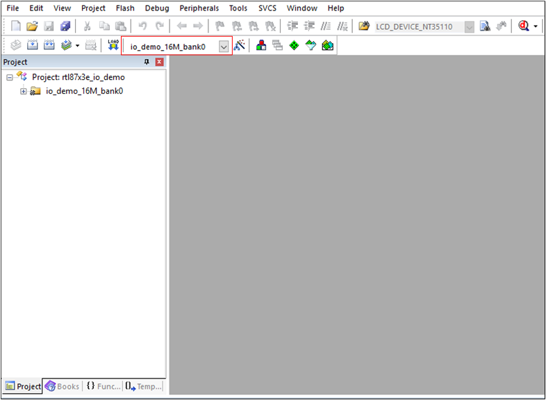
Build the target.

After a successful compilation, the APP bin file
io_demo_bank0_MP-v0.0.0.0-xxx.binwill be generated in the directorybin\rtl87x3e\flash_16M\bank0.Download the generated APP bin
io_demo_bank0_MP-v0.0.0.0-xxx.bininto the EVB board.Press the reset button on the EVB board.
Experimental Verification
The detailed test procedure can be found in the list below:
Code Overview
The IO demo application overview will be introduced according to the following parts:
The IO demo project overview will be introduced in the chapter Source Code Directory.
The IO demo project source code overview will be introduced in the chapter Source Code Overview.
Source Code Directory
IO demo project shows how to use peripherals to communicate with other devices. A specific peripheral and its usage scenario can be changed to demonstrate, with its source files added to the build target and its demo functions called in main().
This section describes the project directory and project structure. The reference files directory is as follows:
Project directory:
board\evb\io_demo.Project source code directory:
src\sample\io_demo.
Source files in the sample project are currently categorized into several groups as below.
└── Project: io_demo_16M_bank0
   ├── include                          ROM UUID header files. Users do not need to modify it.
   ├── lib                              Includes all binary symbol files that user application is built on.
   ├── cmsis                            The cmsis source code. Users do not need to modify it.
   ├── io_driver                        The IO driver code. Users do not need to modify it.
   ├── io_hal                           The IO HAL layer code. Users do not need to modify it.
   ├── app                              The application source code.
   ├── adc                              The ADC demo source code.
   ├── gdma                             The GDMA demo source code.
   ├── gpio                             The GPIO demo source code.
   ├── i2c                              The I2C demo source code.
   ├── ir                               The IR demo source code.
   ├── keyscan                          The KeyScan demo source code. RTL87x3EP doesn’t support it.
   ├── led                              The LED demo source code.
   ├── lpc                              The LPC demo source code.
   ├── qdec                             The QDEC demo source code.
   ├── rtc                              The RTC demo source code.
   ├── sdio                             The SDIO demo source code.
   ├── spi                              The SPI demo source code.
   ├── spi3w                            The 3-wire SPI demo source code. Only RTL87x3D supports it.
   ├── tim                              The TIMER and PWM demo source code.
   ├── uart                             The UART demo source code.
   ├── ctc                              The CapTouch demo source code. Only RTL87x3E supports it.
   ├── i2s                              The I2S demo source code.
   ├── dlps                             The DLPS demo source code.
   └── spi_external_flash               The SPI external flash demo source code.
Source Code Overview
This section describes some parts of the source code used in the application of this project.
Initialization
The main function is invoked when the application is powered on or the chip is reset, and it performs the following initialization functions:
RAM_TEXT_SECTION
int main(void)
{
    __enable_irq();
    WDG_Disable();

    IO_PRINT_INFO0("Hello io demo !");

    extern void gpio_int_demo(void);
    gpio_int_demo();

    os_sched_start();
}
The gpio_int_demo() function can be replaced by the demo entry function in the demo files, such as adc_demo() in the adc_demo.c file. Note that each demo entry function is independent of each other.
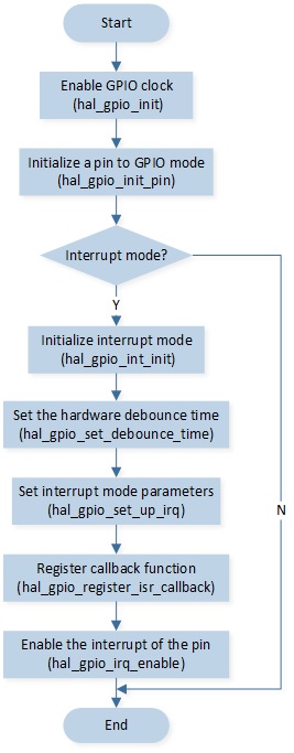
Initialization Flow
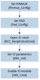
Peripheral initialization mainly consists of the following components:
Set peripheral PINMUX and PAD.
Enable peripheral clock signal.
Set peripheral initialization parameters.
Enable peripheral.
The initialization procedure is shown in the following figure, where ‘XXX’ is the name of the peripheral to be initialized, such as GPIO, I2C, or SPI.
Clock Configuration
Enable GPIO clock by calling RCC_PeriphClockCmd() function.
RCC_PeriphClockCmd(APBPeriph_GPIO, APBPeriph_GPIO_CLOCK, ENABLE);
PINMUX Configuration
Configure PINMUX status of the pin by calling Pinmux_Config() function.
/* Configure Pin P0_5 as GPIO function */
Pinmux_Config(P0_5, DWGPIO);
For optional pin values and map GPIO please reference the file below.
RTL87x3E: inc\rtl87x3e\platform\rtl876x.h
RTL87x3D: inc\rtl87x3d\platform\pin_def.h
RTL87x3EP: inc\rtl87x3ep\platform\pin_def.h
PAD Configuration
Configure the PAD status of the pin by calling Pad_Config() function.
Pad_Config(P0_5, PAD_PINMUX_MODE, PAD_IS_PWRON, PAD_PULL_NONE, PAD_OUT_ENABLE, PAD_OUT_HIGH);
Interrupt Configuration
Enable IRQ interrupt by calling NVIC_Init() function.
NVIC_InitTypeDef NVIC_InitStruct;
NVIC_InitStruct.NVIC_IRQChannel = GPIO5_IRQ;
NVIC_InitStruct.NVIC_IRQChannelPriority = 5;
NVIC_InitStruct.NVIC_IRQChannelCmd = ENABLE;
NVIC_Init(&NVIC_InitStruct);
Initialize Peripheral
Initialize the peripheral by calling XXX_Init for each peripheral, and ‘XXX’ is the name of the peripheral to be initialized.
GPIOx_Init();
Disable Peripheral
Disable the peripheral by calling XXX_DeInit for each peripheral, and ‘XXX’ is the name of the peripheral to be disabled.
GPIOx_DeInit();
PINMUX and PAD
PAD Demo Code Support List
Demo 1 |
dlps_gpio_wk_demo.c |
|---|---|
Sample Purpose |
Demonstrates how PAD wakes up the system from DLPS mode. |
Brief Introduction |
This sample code demonstrates how PAD wakes up the system. |
File Path |
|
Function Entry |
|
Pin Definition |
|
Hardware Connection |
When the system needs to be woken up, connect M0_0 to GND on EVB. |
Expected Result |
1. Press the reset button on the EVB, the string ‘dlps_store: enter dlps’ will be printed in Debug Analyzer, and the system will enter DLPS mode. |
Function Description
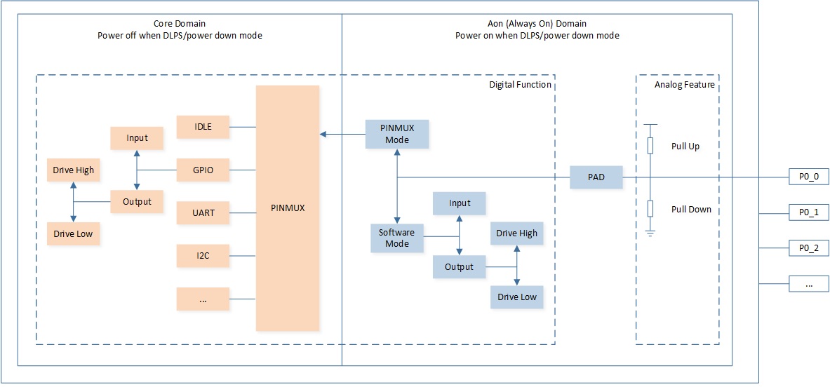
PINMUX is an abbreviation for pin multiplexing. Because the SoC has a limited number of pins, pin multiplexing allows the SoC to use the limited pins for various functions, such as SPI, I2C, and GPIO.
PAD is used to control the behavior of a pin, such as pull-up or pull-down, output high or low level, and wake-up functions.
As shown in the figure below. The PINMUX circuit and IO modules are in the core domain and will be powered down during low power mode, so they cannot work during low power mode. The PAD circuit is in the AON domain and will not be powered down during low power mode, so the PAD can work normally during low power mode. The PAD is mainly used to maintain the pin output state or wake up the system in low power mode.
The PAD can be configured as PINMUX mode and software mode. Only when the PAD is set to PINMUX mode, can this pin be connected to the core domain to achieve pin multiplexing.
PAD Feature List
Two operating modes: PINMUX mode and software mode.
Configurable pin pull-up or pull-down resistors.
Configurable pin independently output high or low level in software mode.
Keep power during DLPS/power down mode, powered off in ship mode.
Wake up the system from DLPS and power down mode from high or low triggers on all the pins.
Hybrid PAD Usage
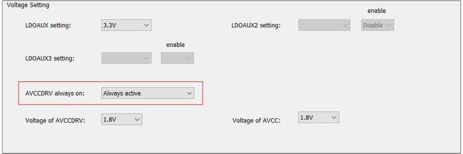
The Hybrid PAD can be configured in digital mode or analog mode. Configure the mode of the hybrid PAD by calling Pad_AnalogMode() function.
/* Configure MIC1_P as analog mode */
Pad_AnalogMode(MIC1_P, PAD_ANALOG_MODE);
When the hybrid PAD is configured in digital mode (GPIO, I2C, etc), the ‘AVCCDRV always on’ option needs to be configured as ‘Always active’ on the MCUConfig Tool.
Note
RTL87x3D hybrid PAD: LOUT_N, P_UART, ROUT_N, ROUT_P, MIC1_N, MIC1_P, MIC2_N, MIC2_P, MIC3_N, MIC3_P, MIC4_N, MIC4_P, MIC5_N, MIC5_P, MIC6_N, MIC6_P, AUX_R, AUX_L, MICBIAS.
RTL87x3E hybrid PAD: AUX_R, AUX_L, MIC1_P, MIC1_N, MIC2_P, MIC2_N, MICBIAS, LOUT_P, LOUT_N, ROUT_P, ROUT_N, MIC3_P, MIC3_N.
RTL87x3EP hybrid PAD: DAOUT_P, DAOUT_N, MIC1_P, MIC1_N, MIC2_P, MIC2_N, MICBIAS.
GPIO
GPIO Demo Code Support List
Demo 1 |
gpio_input_demo.c |
|---|---|
Sample Purpose |
Demonstrates GPIO input mode. |
Brief Introduction |
This sample code demonstrates how to get the input level value of GPIO. |
File Path |
|
Function Entry |
|
GPIO Direction |
Input mode |
Pin Definition |
|
Expected Result |
Press the reset button on the EVB, the string ‘gpio_test: gpio_value 1’ will be printed in Debug Analyzer. |
Demo 2 |
gpio_output_demo.c |
|---|---|
Sample Purpose |
Demonstrates GPIO output mode. |
Brief Introduction |
This sample code demonstrates how to use GPIO to output high and low levels. |
File Path |
|
Function Entry |
|
GPIO Direction |
Output mode |
Hardware Connection |
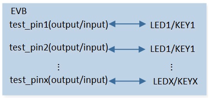
As shown in GPIO Hardware Connection Diagram. On EVB, connect P0_1 and LED1, and connect P0_2 and LED2. |
Pin Definition |
|
Expected Result |
Press the reset button on the EVB. LED1 and LED2 will light up or off when the output level is selected as high or low. |
Demo 3 |
gpioab_output_demo.c |
|---|---|
Sample Purpose |
Demonstrates GPIOx output mode whether the pin belongs to GPIOA or B. |
Brief Introduction |
This sample code demonstrates the GPIOx output function. The output level value can be detected by connecting with LED. |
File Path |
|
Function Entry |
|
GPIO Direction |
Output mode |
Hardware Connection |
As shown in GPIO Hardware Connection Diagram. On EVB, connect P4_3 and LED1. |
Pin Definition |
|
Expected Result |
Press the reset button on the EVB. LED1 will light up or off when the gpio_pin_bit is selected to Set or Reset. |
Demo 4 |
gpioab_output_group_demo.c |
|---|---|
Sample Purpose |
Demonstrates GPIOx group output mode whether the pins belong to GPIOA or B. |
Brief Introduction |
This sample code demonstrates the GPIOx group output function. These output level values can be detected by connecting with LED. |
File Path |
|
Function Entry |
|
GPIO Direction |
Output mode |
Hardware Connection |
As shown in GPIO Hardware Connection Diagram. On EVB, connect LED and test pin. |
Expected Result |
Press the reset button on the EVB. The LED will light up or off when the gpio_pin_bit is selected to Set or Reset. |
Demo 5 |
gpio_int_demo.c |
|---|---|
Sample Purpose |
Demonstrates GPIO used as a key by edge trigger mode with hardware debounce. |
Brief Introduction |
This sample code demonstrates the detection of GPIO input through interrupt. When the button is pressed (such as P1_0 changing from high level to low level), the falling edge of GPIO is detected, and the GPIO interrupt is triggered. Then switch the edge trigger, after the button is released (P1_0 changes from low level to high level), the GPIO interrupt is triggered again. |
File Path |
|
Function Entry |
|
GPIO Direction |
Input mode |
Hardware Connection |
As shown in GPIO Hardware Connection Diagram. On EVB, connect P1_0, P1_1, P2_1, P2_2 to KEY1 ~ KEY4 respectively. |
Pin Definition |
|
Expected Result |
Press the reset button on the EVB. Press KEY1 ~ KEY4: string ‘gpio_isr_cb: pin_name P1_0, gpio_level 0’ ‘gpio_isr_cb: pin_name P1_1, gpio_level 1’ ‘gpio_isr_cb: pin_name P2_1, gpio_level 0’ ‘gpio_isr_cb: pin_name P2_2, gpio_level 1’ will be printed in Debug Analyzer. Release KEY1 ~ KEY4: string ‘gpio_isr_cb: pin_name P1_0, gpio_level 1’ ‘gpio_isr_cb: pin_name P1_1, gpio_level 0’ ‘gpio_isr_cb: pin_name P2_1, gpio_level 1’ ‘gpio_isr_cb: pin_name P2_2, gpio_level 0’ will be printed in Debug Analyzer. |
Demo 6 |
pad_int_demo.c |
|---|---|
Sample Purpose |
Demonstrates PAD interrupt mode to realize key detection. |
Brief Introduction |
This sample code demonstrates key detection by PAD interrupt mode. When the button is pressed (such as P1_0 changing from high level to low level), the low level of the pin is detected, and the system handler is triggered. Then switch the level trigger, after the button is released (P1_0 changes from low level to high level), the system handler is triggered again. |
File Path |
|
Function Entry |
|
GPIO Direction |
Input mode |
Hardware Connection |
As shown in GPIO Hardware Connection Diagram. On EVB, connect P1_0, P1_1, P2_1, P2_2 to KEY1 ~ KEY4 respectively. |
Pin Definition |
|
Expected Result |
Press the reset button on the EVB. Press KEY1: string ‘system_handler: pin0 interrupt triggered, pin_0_state 0’ will be printed in Debug Analyzer. Release KEY1: string ‘system_handler: pin0 interrupt triggered, pin_0_state 1’ will be printed in Debug Analyzer. |
Demo 7 |
gpio_key.c |
|---|---|
Sample Purpose |
Demonstrates GPIO used as a key by level trigger mode with TIMER debounce. |
Brief Introduction |
This sample code demonstrates the detection of GPIO input through interrupt. When the button is pressed (P0_0 changes from high level to low level), the low level of GPIO is detected, and the GPIO interrupt is triggered. Then restart the TIMER in the GPIO handler, after the 30ms debounce time, enter the TIMER handler to switch the level trigger, when the button is released (P1_0 changes from low level to high level), the GPIO interrupt is triggered again. Then the TIMER restarts again. |
File Path |
|
Function Entry |
|
GPIO Direction |
Input mode |
Hardware Connection |
As shown in GPIO Hardware Connection Diagram. On EVB, connect P0_0 and KEY1. |
Pin Definition |
|
Expected Result |
Press the reset button on the EVB. Press KEY1: string ‘key_handler: key_status 0’ ‘debounce_hw_timer_callback: Key press’ will be printed in Debug Analyzer. Release KEY1: string ‘key_handler: key_status 1’ ‘debounce_hw_timer_callback: Key release’ will be printed in Debug Analyzer. |
Demo 8 |
gpio_edge_key.c |
|---|---|
Sample Purpose |
Demonstrates GPIO used as a key by edge trigger mode with hardware debounce. |
Brief Introduction |
This sample code demonstrates the detection of GPIO input through interrupt. When the button is pressed (P0_0 changes from high level to low level), the falling edge of GPIO is detected, and the GPIO interrupt is triggered. Then switch the edge trigger, after the button is released (P0_0 changes from low level to high level), the GPIO interrupt is triggered again. |
File Path |
|
Function Entry |
|
GPIO Direction |
Input mode |
Hardware Connection |
As shown in GPIO Hardware Connection Diagram. On EVB, connect P0_0 and KEY1. |
Pin Definition |
|
Expected Result |
Press the reset button on the EVB. Press KEY1: string ‘key_handler: Key press’ will be printed in Debug Analyzer. Release KEY1: string ‘key_handler: Key release’ will be printed in Debug Analyzer. |
Demo 9 |
dma_tim_demo.c |
|---|---|
Sample Purpose |
Demonstrates how GDMA controls GPIO output. |
Brief Introduction |
This sample code demonstrates how to use TIMER to toggle GDMA to control GPIO to output high and low levels of specified lengths. |
File Path |
|
GPIO Direction |
Output mode |
GDMA Direction |
Memory to Peripheral |
Function Entry |
|
Pin Definition |
|
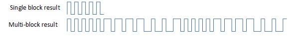
Expected Result |
Press the reset button on the EVB. Use a Logic Analyzer to capture the waveform of P0_2, and the output waveform results of single-block or multi-block are shown in GPIO GDMA Result Diagram. |
Function Description
The GPIO integrated core is programmable general-purpose input/output. Each GPIO pin can be configured by software as an output, input, or interrupt peripheral function.
Feature List
32 independently configured GPIO signals in every port, with independently controllable signal bits.
Support hardware and software control.
Support input and output control.
Support level-triggered and edge-triggered interrupts.
Support low and high level-triggered interrupts.
Support rising and falling edge-triggered interrupts.
Support both-edge-triggered interrupts.
Support hardware debounce function.
Support GPIO+TIMER+GDMA function.
Note
RTL87x3D supports 3 ports. RTL87x3E and RTL87x3EP support 2 ports.
When the GPIO is controlled by GDMA, it should be configured in hardware mode.
GPIO Initialization Flow
The GPIO initialization flow is shown in the following figure.
Input Mode
The codes below demonstrate the operation flow of GPIO in input mode.
hal_gpio_init();
hal_gpio_init_pin(TEST_Pin, GPIO_TYPE_AUTO, GPIO_DIR_INPUT, GPIO_PULL_UP);

gpio_value = hal_gpio_get_input_level(TEST_Pin);
Output Mode
The codes below demonstrate the operation flow of GPIO in output mode.
hal_gpio_init();
hal_gpio_init_pin(TEST_PIN, GPIO_TYPE_CORE, GPIO_DIR_OUTPUT, GPIO_PULL_UP);
hal_gpio_init_pin(TEST_PIN_2, GPIO_TYPE_AON, GPIO_DIR_OUTPUT, GPIO_PULL_UP);

for (uint16_t i = 0; i < 10; i++)
{
    hal_gpio_set_level(TEST_PIN, GPIO_LEVEL_LOW);
    hal_gpio_set_level(TEST_PIN_2, GPIO_LEVEL_LOW);
    hal_gpio_set_level(TEST_PIN, GPIO_LEVEL_HIGH);
    hal_gpio_set_level(TEST_PIN_2, GPIO_LEVEL_HIGH);
}
Interrupt Mode
The codes below demonstrate the operation flow of GPIO in interrupt mode.
hal_gpio_init();
hal_gpio_int_init();
hal_gpio_set_debounce_time(30);

hal_gpio_init_pin(GPIO_DEMO_INPUT_PIN0, GPIO_TYPE_AUTO, GPIO_DIR_INPUT, GPIO_PULL_UP);
hal_gpio_init_pin(GPIO_DEMO_INPUT_PIN1, GPIO_TYPE_AUTO, GPIO_DIR_INPUT, GPIO_PULL_DOWN);
hal_gpio_init_pin(GPIO_DEMO_INPUT_PIN2, GPIO_TYPE_AUTO, GPIO_DIR_INPUT, GPIO_PULL_UP);
hal_gpio_init_pin(GPIO_DEMO_INPUT_PIN3, GPIO_TYPE_AUTO, GPIO_DIR_INPUT, GPIO_PULL_DOWN);

hal_gpio_set_up_irq(GPIO_DEMO_INPUT_PIN0, GPIO_IRQ_EDGE, GPIO_IRQ_ACTIVE_LOW, true);
hal_gpio_set_up_irq(GPIO_DEMO_INPUT_PIN1, GPIO_IRQ_EDGE, GPIO_IRQ_ACTIVE_HIGH, true);
hal_gpio_set_up_irq(GPIO_DEMO_INPUT_PIN2, GPIO_IRQ_EDGE, GPIO_IRQ_ACTIVE_LOW, true);
hal_gpio_set_up_irq(GPIO_DEMO_INPUT_PIN3, GPIO_IRQ_EDGE, GPIO_IRQ_ACTIVE_HIGH, true);

hal_gpio_register_isr_callback(GPIO_DEMO_INPUT_PIN0, gpio_isr_cb, GPIO_DEMO_INPUT_PIN0);
hal_gpio_register_isr_callback(GPIO_DEMO_INPUT_PIN1, gpio_isr_cb, GPIO_DEMO_INPUT_PIN1);
hal_gpio_register_isr_callback(GPIO_DEMO_INPUT_PIN2, gpio_isr_cb, GPIO_DEMO_INPUT_PIN2);
hal_gpio_register_isr_callback(GPIO_DEMO_INPUT_PIN3, gpio_isr_cb, GPIO_DEMO_INPUT_PIN3);

hal_gpio_irq_enable(GPIO_DEMO_INPUT_PIN0);
hal_gpio_irq_enable(GPIO_DEMO_INPUT_PIN1);
hal_gpio_irq_enable(GPIO_DEMO_INPUT_PIN2);
hal_gpio_irq_enable(GPIO_DEMO_INPUT_PIN3);
TIMER and PWM
TIMER and PWM Demo Code Support List
Demo 1 |
tim_demo.c |
|---|---|
Sample Purpose |
Demonstrates how TIMER module works in reload mode and it will trigger the interrupt every 3 seconds. |
File Path |
|
Function Entry |
|
Timeout |
3 seconds |
Expected Result |
Print string ‘demo_hw_timer_callback’ in Debug Analyzer every 3 seconds. |
Demo 2 |
pwm_demo.c |
|---|---|
Sample Purpose |
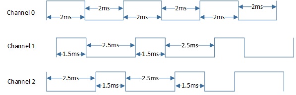
Demonstrates PWM output, PWM complementary output, and deadzone. |
File Path |
|
Function Entry |
|
Pin Definition |
|
Hardware Connection |
Connect M0_0 of EVB to channel 0 of the logic analyzer, connect M0_2 of EVB to channel 1 of the logic analyzer, and connect M0_3 of EVB to channel 2 of the logic analyzer. |
Expected Result |
The waveforms displayed by channels 0/1/2 of the logic analyzer are shown in PWM Demo Expected Result Diagram. |
Demo 3 |
led_demo_task.c |
|---|---|
Sample Purpose |
Demonstrates how to achieve the effect of breath and blink LED with PWM. |
File Path |
|
Function Entry |
|
Pin Definition |
|
Hardware Connection |
On EVB, connect M2_1 to LED0, connect M2_2 to LED1, and connect M2_7 to LED2. |
Expected Result |
LEDs turn from dark to bright and then from bright to dark with the effect of breath light. |
Function Description
The TIMER consists of a 32-bit automatic load counter. Each TIMER is completely independent and does not share any resources. They can operate synchronously together. The TIMER can operate in two modes: user-defined count mode and free-running mode. In user-defined count mode, the TIMER counts down from the value set by the user. In free-running mode, the TIMER counts down from 0xffffffff. When the TIMER counter is enabled after being reset or disabled, the TIMER counts down from its initial value, and when it reaches 0, an interrupt is triggered.
Feature List
Two operation modes: user-defined count mode and free-running mode.
TIMER counter width: 32 bits.
Support PWM output mode.
TIMER 2 and TIMER 3 support PWM complementary output mode.
TIMER 2 and TIMER 3 support deadzone.
TIMER 2 and TIMER 3 support emergency stop control.
Note
RTL87x3D supports up to 16 TIMER, 12 of which can be used for application.
RTL87x3E supports up to 8 TIMER, 5 of which can be used for application.
RTL87x3EP supports up to 12 TIMER, 9 of which can be used for application, but only 5 of which can be used for the PWM function.
TIMER 0 and TIMER 1 are reserved for low stack. TIMER 7 is reserved for log time stamp.
TIMER Operation Flow
The codes below demonstrate the TIMER operation flow. For details, please refer to src\sample\io_demo\tim\interrupt\tim_demo.c.
void tim_driver_init(void)
{
    /* Create the timer, user-defined mode, the period is 3 seconds. */
    demo_timer_handle = hw_timer_create("demo_hw_timer", 3000 * 1000, true, demo_hw_timer_callback);
    if (demo_timer_handle == NULL)
    {
        IO_PRINT_ERROR0("tim_driver_init: fail to create hw timer, check hw timer usage");
        return;
    }

    IO_PRINT_TRACE1("tim_driver_init: create hw timer instance successfully, id %d",
                    hw_timer_get_id(demo_timer_handle));

    /* Start the specified timer */
    hw_timer_start(demo_timer_handle);
}
When the TIMER counter reaches to zero, the interrupt will be triggered and the callback will be executed. The codes below demonstrate the TIMER callback handle flow.
void demo_hw_timer_callback(T_HW_TIMER_HANDLE handle)
{
    //Add User code here
    IO_PRINT_TRACE0("demo_hw_timer_callback");
}
PWM Operation Flow
The codes below demonstrate the PWM operation flow. For details, please refer to src\sample\io_demo\tim\pwm\pwm_demo.c.
static void driver_pwm_init(void)
{
    T_PWM_CONFIG demo_pwm_deadzone_para;

    /* Create the PWM, high-level time is 2 seconds, low-level time is 2 seconds */
    demo_pwm_handle = pwm_create("demo_pwm", PWM_HIGH_LEVEL_CNT, PWM_LOW_LEVEL_CNT, false);
    if (demo_pwm_handle == NULL)
    {
        IO_PRINT_ERROR0("driver_pwm_init: Fail to create pwm handle");
        return;
    }

    /* Configure PIN ADC_0 as PWM output */
    pwm_pin_config(demo_pwm_handle, PWM_OUT_PIN, PWM_FUNC);
    /* Start the specified PWM */
    pwm_start(demo_pwm_handle);

    /* Create the PWM, deadzone is enabled. */
    demo_pwm_deadzone_handle = pwm_create("demo_pwm_deadzone", PWM_HIGH_LEVEL_CNT, PWM_LOW_LEVEL_CNT,
                                          true);
    if (demo_pwm_deadzone_handle == NULL)
    {
        IO_PRINT_ERROR0("driver_pwm_init: Fail to create pwm deadzone handle");
        return;
    }

    /* Set high-level time */
    demo_pwm_deadzone_para.pwm_high_count = PWM_HIGH_LEVEL_CNT;
    /* Set low-level time */
    demo_pwm_deadzone_para.pwm_low_count = PWM_LOW_LEVEL_CNT;
    /* Enable deadzone */
    demo_pwm_deadzone_para.pwm_deadzone_enable = ENABLE;
    /* Configure PWM clock source as 1MHz */
    demo_pwm_deadzone_para.clock_source = PWM_CLOCK_1M;
    /* Set deadzone size count, count frequency is 32K */
    demo_pwm_deadzone_para.pwm_deadzone_size = PWM_DEADZONE_SIZE_CNT;
    /* Configure PWM_P emergency stop state as low-level */
    demo_pwm_deadzone_para.pwm_p_stop_state = PWM_DEAD_ZONE_STOP_LOW;
    /* Configure PWM_N emergency stop state as high-level */
    demo_pwm_deadzone_para.pwm_n_stop_state = PWM_DEAD_ZONE_STOP_HIGH;
    /* Initialize PWM */
    pwm_config(demo_pwm_deadzone_handle, &demo_pwm_deadzone_para);

    /* Configure PIN ADC_2 as PWM_P output */
    pwm_pin_config(demo_pwm_deadzone_handle, PWM_OUT_PIN_P, PWM_FUNC_P);
    /* Configure PIN ADC_3 as PWM_N output */
    pwm_pin_config(demo_pwm_deadzone_handle, PWM_OUT_PIN_N, PWM_FUNC_N);
    /* Start the specified PWM */
    pwm_start(demo_pwm_deadzone_handle);
}
UART
UART Demo Code Support List
Demo 1 |
uart_polling_demo.c |
|---|---|
Sample Purpose |
Demonstrate how UART sends and receives data in polling mode. |
Brief Introduction |
This sample code demonstrates the communication between chip and PC. PC transmits some data to chip and then chip returns the same data received to PC. |
File Path |
|
Function Entry |
|
Hardware Connection |
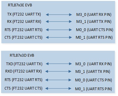
As shown in UART Demo 1/2/3/5 Hardware Connection Diagram. |
UART TX Pin Definition |
|
UART RX Pin Definition |
|
UART ID |
UART0 |
Baud Rate |
115200 |
Parity Check |
No Parity |
Data Format |
8-Bit |
Stop Bit |
1-Bit |
Hardware Flow Control |
None |
Expected Result |
1. Press the reset button on the EVB, string ‘### Welcome to use RealTek Bumblebee ###\r\n’ will be displayed in UART debug tool. |
Demo 2 |
uart_demo.c |
|---|---|
Sample Purpose |
Demonstrate how UART receives data in interrupt mode. |
Brief Introduction |
This sample code demonstrates the communication between chip and PC. PC transmits some data to chip and then chip returns the same data received to PC. |
File Path |
|
Function Entry |
|
Hardware Connection |
As shown in UART Demo 1/2/3/5 Hardware Connection Diagram. |
UART TX Pin Definition |
|
UART RX Pin Definition |
|
UART ID |
UART0 |
Baud Rate |
115200 |
Parity Check |
No Parity |
Data Format |
8-Bit |
Stop Bit |
1-Bit |
Hardware Flow Control |
None |
Expected Result |
1. Press the reset button on the EVB, string ‘### Welcome to use RealTek Bumblebee ###\r\n’ will be displayed in UART debug tool. |
Demo 3 |
uart_tx_demo.c |
|---|---|
Sample Purpose |
Demonstrate how UART sends data in interrupt mode. |
Brief Introduction |
This sample code demonstrates the communication between chip and PC. Chip transmits some data to PC. |
File Path |
|
Function Entry |
|
Hardware Connection |
As shown in UART Demo 1/2/3/5 Hardware Connection Diagram. |
UART TX Pin Definition |
|
UART RX Pin Definition |
|
UART ID |
UART0 |
Baud Rate |
115200 |
Parity Check |
No Parity |
Data Format |
8-Bit |
Stop Bit |
1-Bit |
Hardware Flow Control |
None |
Expected Result |
Press the reset button on the EVB, string ‘### Welcome to use RealTek Bumblebee ###\r\n’ will be displayed in UART debug tool. |
Demo 4 |
uart_fc_demo.c |
|---|---|
Sample Purpose |
Demonstrate how UART sends and receives data with hardware flow control. |
Brief Introduction |
This sample code demonstrates the communication between chip and PC. PC transmits some data to chip and then chip returns the same data received to PC. |
File Path |
|
Function Entry |
|
Hardware Connection |
As shown in UART Demo 4 Hardware Connection Diagram. |
UART TX Pin Definition |
|
UART RX Pin Definition |
|
UART CTS Pin Definition |
|
UART RTS Pin Definition |
|
UART ID |
UART0 |
Baud Rate |
115200 |
Parity Check |
No Parity |
Data Format |
8-Bit |
Stop Bit |
1-Bit |
Hardware Flow Control |
CTS and RTS Flow Control. |
Expected Result |
1. Press the reset button on the EVB, string ‘### Uart demo–Auto Hardware Flow Contrl ###\r\n’ will be displayed in UART debug tool. |
Demo 5 |
dlps_uart_demo.c |
|---|---|
Sample Purpose |
Demonstrates how UART wakes up the system from DLPS mode. |
Brief Introduction |
This sample code demonstrates the communication between chip and PC. It realizes the function that transmits and receives data through UART and wakes up the system by UART after entering DLPS mode. System will enter DLPS mode automatically while it is in idle state. When some data is sent to chip, |
File Path |
|
Function Entry |
|
Hardware Connection |
As shown in UART Demo 1/2/3/5 Hardware Connection Diagram. |
UART TX Pin Definition |
|
UART RX Pin Definition |
|
UART ID |
UART2 |
Baud Rate |
115200 |
Parity Check |
No Parity |
Data Format |
8-Bit |
Stop Bit |
1-Bit |
Hardware Flow Control |
None |
Expected Result |
1. Press the reset button on the EVB, string ‘### Welcome to use RealTek Bumblebee ###\r\n’ will be displayed in UART debug tool. |
Demo 6 |
adp_1wire_uart_demo.c |
|---|---|
Sample Purpose |
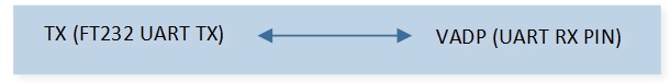
Demonstrates how adapter one-wire works. |
Brief Introduction |
This sample code demonstrates how adapter one-wire works. When the adapter plugs in, it works as UART RX. When the adapter plugs out, it works as GPIO. |
File Path |
|
Function Entry |
|
Hardware Connection |
As shown in UART Demo 6 Hardware Connection Diagram. On EVB, TX of FT232 is connected to VADP. |
UART RX Pin Definition |
RTL87x3D: |
UART ID |
UART0 |
Baud Rate |
9600 |
Parity Check |
No Parity |
Data Format |
8-Bit |
Stop Bit |
1-Bit |
Hardware Flow Control |
None |
Expected Result |
1. Press the reset button on the EVB. |

Function Description
UART provides a flexible method for full-duplex data exchange with external devices. The UART utilizes a fractional baud rate generator to provide a wide range of baud rate options. It supports half-duplex single-wire communication. UART can also be used with GDMA to achieve high-speed data communication..
Feature List
Support 1-bit or 2-bit stop bit.
Support 7-bit or 8-bit data format.
Support odd or even parity.
Support hardware flow control.
Programmable baud rate.
Support GDMA.
Support one-wire UART.
Note
RTL87x3D supports 4 UART. RTL87x3E and RTL87x3EP support 3 UART. UART1 is used as log UART.
Data Format
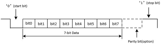
The schematic diagram of the 7-bit data format is shown in the following figure.
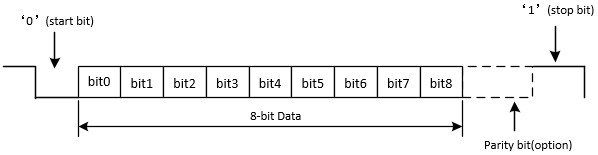
The schematic diagram of the 8-bit data format is shown in the following figure.
Parity Check
Odd Parity
Odd parity means that the number of ‘1’ in the data bits and check bit is odd. When the number of ‘1’ in the data bits is odd, the check bit is ‘0’; otherwise, it is ‘1’.
Even Parity
Even parity means that the number of ‘1’ in the data bits and check bit is even. When the number of ‘1’ in the data bits is even, the check bit is ‘0’; otherwise, it is ‘1’.
Hardware Flow Control
The schematic diagram of hardware flow control is shown in the following figure.
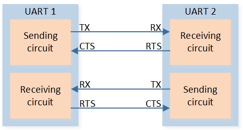
RTS Flow Control
When the UART receiver is ready to accept new data, RTS becomes valid, and the low level is valid. When the number of data in the RX FIFO reaches the set RX trigger level, RTS becomes invalid (high level is invalid), thereby indicating that it is desired to stop data transmission at the end of the current frame.
CTS Flow Control
The transmitter checks the CTS before sending the next frame. If CTS is valid (low level is valid), the next data is sent; otherwise, the next frame data is not sent. If the CTS becomes invalid (high level is invalid) during transmission, the transmission is stopped after the current transmission is completed.
Baud Rate
Set the baud rate by configuring the variables div, ovsr, and ovsr_adj. UART baud rate table is shown below.
Baud Rate |
Variable div |
Variable ovsr |
Variable ovsr_adj |
|---|---|---|---|
1200 |
2589 |
7 |
0x7F7 |
9600 |
271 |
10 |
0x24A |
14400 |
271 |
5 |
0x222 |
19200 |
123 |
11 |
0x6FF |
28800 |
82 |
11 |
0x6FF |
38400 |
85 |
7 |
0x222 |
57600 |
41 |
11 |
0x6FF |
76800 |
35 |
9 |
0x7EF |
115200 |
20 |
12 |
0x252 |
128000 |
25 |
7 |
0x555 |
153600 |
15 |
12 |
0x252 |
230400 |
10 |
12 |
0x252 |
460800 |
5 |
12 |
0x252 |
500000 |
8 |
5 |
0 |
921600 |
3 |
9 |
0x2AA |
1000000 |
4 |
5 |
0 |
1382400 |
2 |
9 |
0x2AA |
1444400 |
2 |
8 |
0x5F7 |
1500000 |
2 |
8 |
0x492 |
1843200 |
2 |
5 |
0x3F7 |
2000000 |
2 |
5 |
0 |
2100000 |
2 |
14 |
0x400 |
2764800 |
1 |
9 |
0x2AA |
3000000 |
1 |
8 |
0x492 |
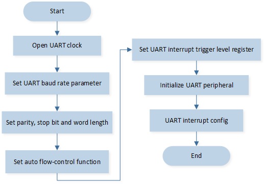
Initialization Flow
UART initialization flow is shown in the following figure.
The codes below demonstrate the UART interrupt handle flow.
/* Enable UART0 clock */
RCC_PeriphClockCmd(APBPeriph_UART0, APBPeriph_UART0_CLOCK, ENABLE);

UART_InitTypeDef uartInitStruct;
/* Fill each UART_InitTypeDef member variable with its default value */
UART_StructInit(&uartInitStruct);

/* Change default rx trigger level */
uartInitStruct.rxTriggerLevel = UART_RX_FIFO_TRIGGER_LEVEL_14BYTE;

UART_Init(UART0, &uartInitStruct);

//enable rx interrupt and line status interrupt
UART_INTConfig(UART0, UART_INT_RD_AVA | UART_INT_LINE_STS | UART_INT_IDLE, ENABLE);

RamVectorTableUpdate(UART0_VECTORn, (IRQ_Fun)Data_Uart_Handler);

NVIC_InitTypeDef NVIC_InitStruct;
NVIC_InitStruct.NVIC_IRQChannel = UART0_IRQn;
NVIC_InitStruct.NVIC_IRQChannelPriority = 3;
NVIC_InitStruct.NVIC_IRQChannelCmd = ENABLE;
NVIC_Init(&NVIC_InitStruct);
Receive Data by Interrupt Mode
UART interrupt handle flow is shown in the following figure.
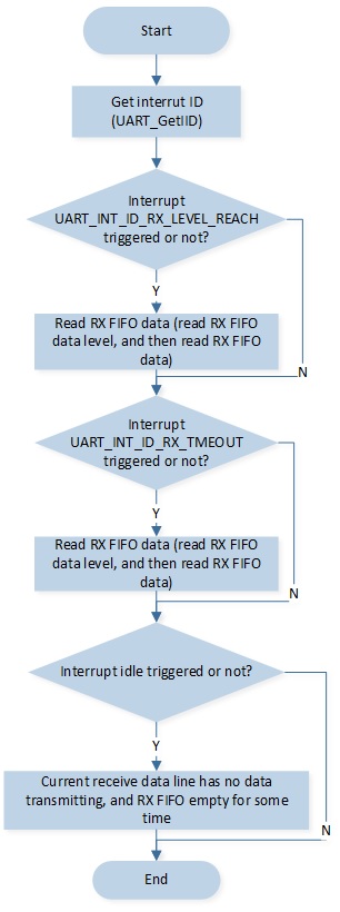
The codes below demonstrate the UART interrupt handle flow.
void data_uart_handler(void)
{
    uint8_t event = IO_DEMO_EVENT_UART_RX;
    uint32_t int_status = 0;
    uint8_t recv_len;
    uint8_t line_status = 0;

    if (UART_GetFlagState(UART0, UART_FLAG_RX_IDLE) == SET)
    {
        UART_INTConfig(UART0, UART_INT_IDLE, DISABLE);
        if (os_msg_send(io_queue_handle, &event, 0) == false)
        {
            IO_PRINT_ERROR0("data_uart_handler: Send Queue Error");
        }
        //user code here

        UART_INTConfig(UART0, UART_INT_IDLE, ENABLE);
    }

    /* read interrupt id */
    int_status = UART_GetIID(UART0);

    switch (int_status)
    {
    /* tx fifo empty, not enable */
    case UART_INT_ID_TX_EMPTY:
        break;

    /* rx data available */
    case UART_INT_ID_RX_LEVEL_REACH:
        recv_len = UART_GetRxFIFOLen(UART0);
        UART_ReceiveData(UART0, &RxBuffer[RxCount], recv_len);
        RxCount += recv_len;
        break;

    case UART_INT_ID_RX_TMEOUT:
        recv_len = UART_GetRxFIFOLen(UART0);
        UART_ReceiveData(UART0, &RxBuffer[RxCount], recv_len);
        RxCount += recv_len;

        break;

    /* receive line status interrupt */
    case UART_INT_ID_LINE_STATUS:
        line_status = UART_GetLineStatus(UART0);
        IO_PRINT_ERROR1("data_uart_handler: line_status 0x%x", line_status);
        UART_SendByte(UART0, line_status);
        break;

    default:
        break;
    }

    return;
}
Send Data
UART interrupt handle flow is shown in the following figure.
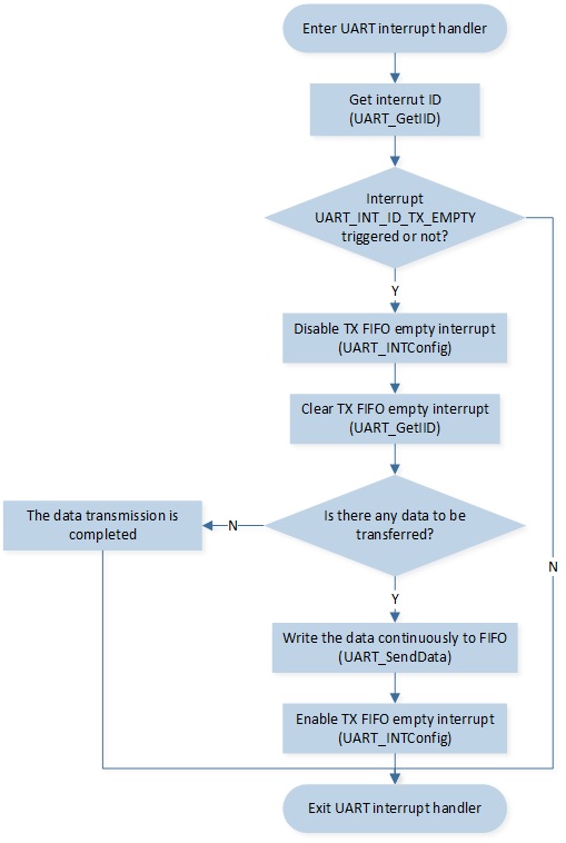
The codes below demonstrate the UART interrupt handle flow.
static void uart_send_data(uint8_t *buf, uint32_t len)
{
    uint32_t tx_len = len > UART_TX_FIFO_SIZE ? UART_TX_FIFO_SIZE : len;

    UART_SendData(UART0, buf, tx_len);

    uart_tx_curr_addr = buf + tx_len;
    uart_tx_len = len - tx_len;

    UART_INTConfig(UART0, UART_INT_FIFO_EMPTY, ENABLE);
}

static void uart0_interrupt_handler(void)
{
    uint32_t int_status = 0;

    /* read interrupt id */
    int_status = UART_GetIID(UART0);

    switch (int_status)
    {
    /* tx fifo empty */
    case UART_INT_ID_TX_EMPTY:
        UART_INTConfig(UART0, UART_INT_FIFO_EMPTY, DISABLE);
        UART_GetIID(UART0);
        if (uart_tx_len)
        {
            uart_send_data(uart_tx_curr_addr, uart_tx_len);
        }
        break;

    /* rx data available */
    case UART_INT_ID_RX_LEVEL_REACH:
        break;

    case UART_INT_ID_RX_TMEOUT:
        break;

    /* receive line status interrupt */
    case UART_INT_ID_LINE_STATUS:
        break;

    default:
        break;
    }
    return;
}
GDMA
GDMA Demo Code Support List
Demo 1 |
gdma_demo.c |
|---|---|
Sample Purpose |
Demonstrate memory to memory by GDMA. |
Brief Introduction |
This sample code demonstrates memory to memory by GDMA. The data in |
File Path |
|
Function Entry |
|
GDMA DIR |
|
GDMA BufferSize |
100 |
GDMA SourceInc |
|
GDMA DestinationInc |
|
GDMA SourceDataSize |
|
GDMA DestinationDataSize |
|
GDMA SourceMsize |
|
GDMA DestinationMsize |
|
GDMA SourceAddr |
|
GDMA DestinationAddr |
|
Expected Result |
1. Press the reset button on the EVB. |
Demo 2 |
dma_multiblock_demo.c |
|---|---|
Sample Purpose |
Demonstrate how GDMA multi-block function works. |
Brief Introduction |
This sample code demonstrates how GDMA multi-block function works. The data in |
File Path |
|
Function Entry |
|
GDMA DIR |
|
GDMA BufferSize |
100 |
GDMA SourceInc |
|
GDMA DestinationInc |
|
GDMA SourceDataSize |
|
GDMA DestinationDataSize |
|
GDMA SourceMsize |
|
GDMA DestinationMsize |
|
GDMA SourceAddr |
|
GDMA DestinationAddr |
|
GDMA Multi-Block Mode |
|
Expected Result |
1. Press the reset button on the EVB. |
Demo 3 |
dma_scrgar_demo.c |
|---|---|
Sample Purpose |
Demonstrate memory to memory transfer by scatter/gather GDMA. |
Brief Introduction |
This sample code demonstrates how GDMA scatter/gather function works. The data in |
File Path |
|
Function Entry |
|
GDMA DIR |
|
GDMA BufferSize |
20 |
GDMA SourceInc |
|
GDMA DestinationInc |
|
GDMA SourceDataSize |
|
GDMA DestinationDataSize |
|
GDMA SourceMsize |
|
GDMA DestinationMsize |
|
GDMA SourceAddr |
|
GDMA DestinationAddr |
|
GDMA Scatter Mode |
|
GDMA Scatter Count |
4 |
GDMA Scatter Interval |
4 |
Expected Result |
1. Press the reset button on the EVB. |
Demo 4 |
uart_rx_dma.c |
|---|---|
Sample Purpose |
Demonstrate how UART receives data by GDMA. |
Brief Introduction |
This sample code demonstrates the communication between chip and PC. PC transmits some data to chip. |
File Path |
|
Function Entry |
|
Hardware Connection |
As shown in UART Demo 1/2/3/5 Hardware Connection Diagram. |
UART TX Pin Definition |
|
UART RX Pin Definition |
|
UART ID |
UART0 |
Baud Rate |
3000000 |
Parity Check |
No Parity |
Data Format |
8-Bit |
Stop Bit |
1-Bit |
Hardware Flow Control |
None |
Expected Result |
1. Press the reset button on the EVB, string ‘### Welcome to use RealTek Bumblebee ###\r\n’ will be displayed in UART debug tool. |
Demo 5 |
uart_tx_gdma.c |
|---|---|
Sample Purpose |
Demonstrate how UART sends data by GDMA. |
Brief Introduction |
This sample code demonstrates the communication between chip and PC. Chip transmits some data to PC. |
File Path |
|
Function Entry |
|
Hardware Connection |
As shown in UART Demo 1/2/3/5 Hardware Connection Diagram. |
UART TX Pin Definition |
|
UART RX Pin Definition |
|
UART ID |
UART0 |
Baud Rate |
115200 |
Parity Check |
No Parity |
Data Format |
8-Bit |
Stop Bit |
1-Bit |
Hardware Flow Control |
None |
Expected Result |
Press the reset button on the EVB, string ‘### Welcome to use RealTek Bumblebee ###\r\n’ will be displayed in UART debug tool. |
Demo 6 |
adc_gdma_demo.c |
|---|---|
Sample Purpose |
Demonstrate how ADC samples data in continuous mode by GDMA. |
Brief Introduction |
Use continuous mode of ADC peripheral to measure voltage on P0_0 and P0_1. |
File Path |
|
Function Entry |
|
Pre-Condition |
Turn off ‘Charger auto enable’ and ‘Battery detection support’ on the MCUConfig Tool. |
Channel |
ADC0 |
External Channel Input Mode |
ADC0 and ADC1 are divide mode. |
Hardware Connection |
Connect M0_0 and M0_1 of EVB to external DC voltage source. Input voltage of M0_0 and M0_1 must range from 0 to 3.3V. |
Expected Result |
Press the reset button on the EVB, ADC starts continuous sampling, and sample rawdata will be stored in array |
Demo 7 |
i2c_dma_demo.c |
|---|---|
Sample Purpose |
Demonstrate how I2C master and slave work in GDMA mode. |
Brief Introduction |
This sample code demonstrates the communication between I2C master and slave in GDMA mode. Master will read data from slave. |
File Path |
|
Function Entry |
|
Hardware Connection |
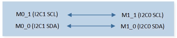
As shown in I2C GDMA Hardware Connection Diagram. On EVB, connect P0_0 to P1_0, connect P0_1 to P1_1. |
I2C Master SCL Pin Definition |
|
I2C Master SDA Pin Definition |
|
I2C Slave SCL Pin Definition |
|
I2C Slave SDA Pin Definition |
|
I2C Master ID |
I2C1 |
I2C Slave ID |
I2C0 |
Clock Speed |
400000 |
Address Mode |
7-Bit |
Slave Address |
0x50 |
ACK |
ACK Enable |
GDMA DIR |
Master: |
GDMA BufferSize |
|
GDMA SourceInc |
Master: |
GDMA DestinationInc |
Master: |
GDMA SourceDataSize |
Master: |
GDMA DestinationDataSize |
Master: |
GDMA SourceMsize |
|
GDMA DestinationMsize |
|
GDMA SourceAddr |
Master: |
GDMA DestinationAddr |
Master: |
GDMA SourceHandshake |
Master: |
GDMA DestHandshake |
Slave: |
Expected Result |
1. Press the reset button on the EVB. |
Demo 8 |
dlps_gdma_recover_demo.c |
|---|---|
Sample Purpose |
Demonstrate how GDMA recovers from DLPS. |
Brief Introduction |
This sample code demonstrates how GDMA recovers from DLPS. The UART can receive data through GDMA when the chip wakes up from DLPS. |
File Path |
|
Function Entry |
|
Hardware Connection |
As shown in GDMA Recover From DLPS Hardware Connection Diagram. |
UART TX Pin Definition |
|
UART RX Pin Definition |
|
UART ID |
UART0 |
Baud Rate |
3000000 |
Parity Check |
No Parity |
Data Format |
8-Bit |
Stop Bit |
1-Bit |
Hardware Flow Control |
None |
Expected Result |
1. Press the reset button on the EVB, string ‘### Welcome to use RealTek Bumblebee ###\r\n’ will be displayed in UART debug tool. |
Demo 9 |
spi_dma_demo.c |
|---|---|
Sample Purpose |
Demonstrate how SPI sends and receives data in master mode by GDMA. |
File Path |
|
Function Entry |
|
Hardware Connection |
As shown in SPI Demo 4 Hardware Connection Diagram. Connect M0_1 to CS of SPI slave device, connect M0_0 to SCK of SPI slave device, connect M1_0 to MISO of SPI slave device, and connect M1_1 to MOSI of SPI slave device. |
SPI CS Pin Definition |
|
SPI SCK Pin Definition |
|
SPI MOSI Pin Definition |
|
SPI MISO Pin Definition |
|
SPI ID |
SPI1 |
Mode |
Master |
Speed |
400000 |
Data Size |
8-Bit |
Expected Result |
1. Press the reset button on the EVB, the data in array sendbuf is sent to SPI slave device and prints the string ‘spi_tx_dma_handler’ in the Debug Analyzer. |
Function Description
GDMA is used to provide high-speed data transfer between peripherals and memory or between memory and memory. The data transfer can be done independently of the CPU to reduce the CPU overhead.
Each channel of the GDMA controller can handle requests from one or more peripherals for memory access. The GDMA controller has an arbitrator to coordinate the priority of each GDMA request.
Feature List
Programmable transfer type for each channel: memory to memory, memory to peripheral, peripheral to memory, peripheral to peripheral.
Programmable source and destination addresses for each channel.
Address increment, or fixed.
Programmable burst transaction size for each channel.
Support transfer abort/suspend function.
Programmable channel priority.
Independent interrupts and control bit for every channel.
Support single-block and multi-block transfer.
Support scatter and gather transfer.
Note
RTL87x3D supports 16 channels, if using SPI high-speed mode, please use channel 0 and 1. RTL87x3E supports 9 channels, RTL87x3EP supports 12 channels.
Parameter Significance
GDMA_ChannelNumChannel numbers can be 0 to 15.
GDMA_DIRThe transfer direction can be memory to memory or memory to peripheral or peripheral to memory or peripheral to peripheral.
GDMA_SourceIncIndicates whether to increment the source address on every source transfer.
GDMA_DestinationIncIndicates whether to increment the destination address on every destination transfer.
GDMA_SourceDataSizeSource single transaction size in bytes:
src_single_size_bytes =
GDMA_SourceDataSizeGDMA_DestinationDataSizeDestination single transaction size in bytes:
dst_single_size_bytes =
GDMA_DestinationDataSizeGDMA_SourceMsizeSource burst transaction size in bytes:
src_burst_size_bytes =
GDMA_SourceMsize* src_single_size_bytesGDMA_DestinationMsizeDestination burst transaction size in bytes:
dst_burst_size_bytes =
GDMA_DestinationMsize* dst_single_size_bytesGDMA_BufferSizeThe total number of bytes to be transferred in a block is:
blk_size_bytes_dma =
GDMA_BufferSize* src_single_size_bytes
Note
The above parameter configuration needs to satisfy the following formula:
GDMA_SourceDataSize * GDMA_SourceMsize = GDMA_DestinationDataSize * GDMA_DestinationMsize
Waterlevel Setting
Handshaking interfaces are used at the transaction level to control the flow of single or burst transactions. Waterlevel is mainly divided into TX FIFO waterlevel and RX FIFO waterlevel. When the effective data amount in the FIFO reaches the set value of waterlevel, a burst transmission is initiated. GDMA_SourceMsize, GDMA_DestinationMsize, GDMA_SourceDataSize, GDMA_DestinationDataSize and peripheral waterlevel setting table is presented below.
IO |
Dir |
Peripheral |
GDMA_ |
GDMA_ |
GDMA_ |
GDMA_ |
|---|---|---|---|---|---|---|
UART |
TX |
.TxWaterlevel |
1 |
4 |
Word |
Byte |
RX |
.RxWaterlevel |
4 |
1 |
Byte |
Word |
|
SPI |
TX |
.SPI_TxWaterlevel |
4 |
8 |
Word |
HalfWord |
RX |
.SPI_RxWaterlevel |
8 |
4 |
HalfWord |
Word |
|
TX |
.SPI_TxWaterlevel |
1 |
4 |
Word |
Byte |
|
RX |
.SPI_RxWaterlevel |
4 |
1 |
Byte |
Word |
|
SPI |
TX |
.SPI_TxWaterlevel |
1 |
4 |
Word |
Byte |
RX |
.SPI_RxWaterlevel |
4 |
1 |
Byte |
Word |
|
I2C |
TX |
.I2C_TxWaterlevel |
4 |
8 |
Word |
HalfWord |
RX |
.I2C_RxWaterlevel |
4 |
1 |
Byte |
Word |
|
ADC |
.adcBurstSize |
8 |
8 |
HalfWord |
HalfWord |
|
SPI_HS |
TX |
.SPI_TxWaterlevel |
32 |
32 |
Byte |
Byte |
RX |
.SPI_RxWaterlevel |
32 |
32 |
Byte |
Byte |
GDMA Single-Block Transfer Initialization Flow
The initialization flow of GDMA single-block transfer is shown in the following figure.
![]()
The codes below demonstrate the GDMA single-block transfer.
uint16_t i = 0;
RCC_PeriphClockCmd(APBPeriph_GDMA, APBPeriph_GDMA_CLOCK, ENABLE);
GDMA_InitTypeDef GDMA_InitStruct;

if (!GDMA_channel_request(&mem_to_mem_dma_ch_num, demo_dma_handler, true))
{
    return;
}

/*--------------initialize test buffer---------------------*/
for (i = 0; i < 100; i++)
{
    GDMA_SendBuffer[i] = (i & 0xff);
}
for (i = 0; i < 100; i++)
{
    GDMA_RecvBuffer[i] = 0;
}

GDMA_StructInit(&GDMA_InitStruct);
GDMA_InitStruct.GDMA_ChannelNum      = DEMO_DMA_CHANNEL_NUM;
GDMA_InitStruct.GDMA_DIR             = GDMA_DIR_MemoryToMemory;
GDMA_InitStruct.GDMA_BufferSize      = 100;//determine total transfer size
GDMA_InitStruct.GDMA_SourceInc       = DMA_SourceInc_Inc;
GDMA_InitStruct.GDMA_DestinationInc  = DMA_DestinationInc_Inc;
GDMA_InitStruct.GDMA_SourceDataSize  = GDMA_DataSize_Byte;
GDMA_InitStruct.GDMA_DestinationDataSize = GDMA_DataSize_Byte;
GDMA_InitStruct.GDMA_SourceMsize      = GDMA_Msize_1;
GDMA_InitStruct.GDMA_DestinationMsize = GDMA_Msize_1;
GDMA_InitStruct.GDMA_SourceAddr      = (uint32_t)GDMA_SendBuffer;
GDMA_InitStruct.GDMA_DestinationAddr = (uint32_t)GDMA_RecvBuffer;
GDMA_Init(DEMO_DMA_CHANNEL, &GDMA_InitStruct);

/*-----------------GDMA IRQ init-------------------*/
NVIC_InitTypeDef nvic_init_struct;
nvic_init_struct.NVIC_IRQChannel         = DEMO_DMA_IRQ;
nvic_init_struct.NVIC_IRQChannelCmd      = (FunctionalState)ENABLE;
nvic_init_struct.NVIC_IRQChannelPriority = 3;
NVIC_Init(&nvic_init_struct);

GDMA_INTConfig(DEMO_DMA_CHANNEL_NUM, GDMA_INT_Block, ENABLE);
GDMA_Cmd(DEMO_DMA_CHANNEL_NUM, ENABLE);
I2C
I2C Demo Code Support List
Demo 1 |
i2c_demo.c |
|---|---|
Sample Purpose |
Demonstrate how I2C writes and reads data in interrupt mode. |
Brief Introduction |
This sample code demonstrates the communication between the chip and I2C slave. The chip writes some data to I2C slave and then chip reads data from I2C slave. |
File Path |
|
Function Entry |
|
Hardware Connection |
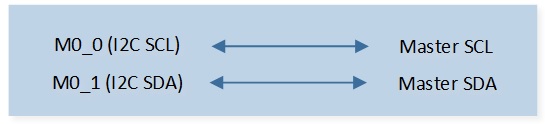
As shown in I2C Demo 1/2/3 Hardware Connection Diagram. On EVB, connect P0_0 to the SCL of the I2C slave, connect P0_1 to the SDA of the I2C slave. |
I2C SCL Pin Definition |
|
I2C SDA Pin Definition |
|
I2C ID |
I2C0 |
Clock Speed |
100000 |
Device Mode |
Master |
Address Mode |
7 Bit |
Slave Address |
0x50 |
ACK |
ACK Enable |
Expected Result |
1. Press the reset button on the EVB, the I2C slave will receive data 0xaa and 0xbb, and the chip will receive four bytes from the I2C slave. |
Demo 2 |
i2c_mw_demo.c |
|---|---|
Sample Purpose |
Demonstrate I2C master write function. |
Brief Introduction |
This sample code demonstrates the I2C master write function. The chip transmits some data to the I2C slave. |
File Path |
|
Function Entry |
|
Hardware Connection |
As shown in I2C Demo 1/2/3 Hardware Connection Diagram. On EVB, connect P0_0 to the SCL of the I2C slave, connect P0_1 to the SDA of the I2C slave. |
I2C SCL Pin Definition |
|
I2C SDA Pin Definition |
|
I2C ID |
I2C1 |
Clock Speed |
400000 |
Device Mode |
Master |
Address Mode |
7 Bit |
Slave Address |
|
ACK |
ACK Enable |
Expected Result |
1. Press the reset button on the EVB, the I2C slave will receive data 0xaa, 0xbb, 0x66, 0x68, 0x77, 0x88. |
Demo 3 |
i2c_polling_demo.c |
|---|---|
Sample Purpose |
Demonstrate how I2C writes and reads data in polling mode. |
Brief Introduction |
This sample code demonstrates the communication between the chip and the I2C slave. The chip writes some data to the I2C slave and then the chip reads data from the I2C slave. |
File Path |
|
Function Entry |
|
Hardware Connection |
As shown in I2C Demo 1/2/3 Hardware Connection Diagram. On EVB, connect P0_0 to the SCL of the I2C slave, connect P0_1 to the SDA of the I2C slave. |
I2C SCL Pin Definition |
|
I2C SDA Pin Definition |
|
I2C ID |
I2C1 |
Clock Speed |
400000 |
Device Mode |
Master |
Address Mode |
7 Bit |
Slave Address |
|
ACK |
ACK Enable |
Expected Result |
1. Press the reset button on the EVB, the I2C slave will receive data 0xaa and 0xbb, and the chip will receive four bytes from the I2C slave. |
Demo 4 |
i2c_slave_demo.c |
|---|---|
Sample Purpose |
Demonstrate how I2C slave works. |
Brief Introduction |
This sample code demonstrates the communication between the chip and I2C master. The chip can read data from the I2C master and write data to the I2C master. |
File Path |
|
Function Entry |
|
Hardware Connection |
As shown in I2C Demo 4 Hardware Connection Diagram. On EVB, connect P0_0 to the SCL of the I2C master. On EVB, connect P0_1 to the SDA of the I2C master. |
I2C SCL Pin Definition |
|
I2C SDA Pin Definition |
|
I2C ID |
I2C1 |
Clock Speed |
100000 |
Device Mode |
Slave |
Address Mode |
7 Bit |
Slave Address |
0x50 |
ACK |
ACK Enable |
Expected Result |
1. Press the reset button on the EVB. |

Function Description
The I2C bus is a two-wire serial interface, consisting of a serial data line (SDA) and a serial clock (SCL). These wires carry information between the devices connected to the bus. Each device is recognized by a unique address and can operate as either a transmitter or receiver, depending on the function of the device. Devices can also be considered masters or slaves when performing data transfers. A master is a device that initiates a data transfer on the bus and generates the clock signals to permit that transfer. At that time, any device addressed is considered a slave.
Feature List
Up to 3 I2C.
Two-wire I2C serial interface: consists of a serial data line (SDA) and a serial clock (SCL).
Support master and slave mode.
Support 7/10-bit addressing mode.
Support standard mode (0 to 100Kb/s).
Support fast mode (less than or equal to 400Kb/s) or fast mode plus (less than or equal to 1000Kb/s).
Interrupt or polling mode operation.
Support GDMA.
I2C Transfer Protocol
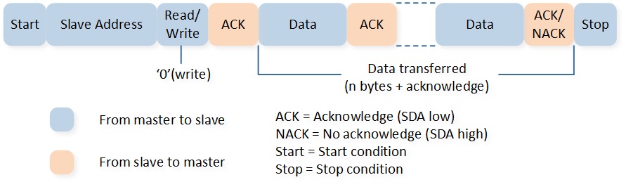
Each byte sent on the SDA line must be 8 bits. There is no limit to the number of bytes that can be sent per transfer, and each byte must be followed by a response bit. The most significant bit (MSB) of the data is transmitted first. If the slave needs to complete some other functions, such as an internal interrupt service routine, it can receive or send the next complete data byte. The clock line SCL can be kept low to force the master to enter the wait state. When the slave is ready to receive the next data byte and release the clock line SCL, the data transfer continues.
![]()
Master Mode
7-Bit Addressing Mode
Master Write
Master-transmitter transmits to slave-receiver with a 7-bit slave address. The transfer direction is not changed. All data is transmitted in byte format, with no limit on the number of bytes transferred per data transfer. After the master sends the address and read/write bit or the master transmits a byte of data to the slave, the slave-receiver must respond with the acknowledge signal (ACK). When a slave-receiver does not respond with an ACK pulse, the master aborts the transfer by issuing a stop condition. The slave must leave the SDA line high so that the master can abort the transfer.
Master Read
In the first response, master-transmitter becomes master-receiver, and slave-receiver becomes slave-transmitter, and the first response is still generated by the slave. If the master is receiving data, the master responds to the slave-transmitter with an acknowledge pulse after a byte of data has been received, except for the last byte. This (NACK) is the way the master-receiver notifies the slave-transmitter that this is the last byte. The slave-transmitter relinquishes the SDA line after detecting the no acknowledge (NACK) so that the master can issue a stop condition.
Master Repeat Read
When performing a write-before-read operation, both the start condition and the slave address are sent repeatedly, but the read/write bit is reversed.
10-Bit Addressing Mode
Master Write
Master-transmitter transmits to slave-receiver with a 10-bit slave address. The transfer direction is not changed.
Master Read
Master-transmitter transmits to slave-receiver with a 10-bit slave address. The transfer direction is changed after the second read/write bit, master-transmitter becomes master-receiver, and slave-receiver becomes slave-transmitter.

Master Repeat Read
The master sends data to the slave and then reads data from the same slave. The transfer direction is changed after the second read/write bit.

I2C Clock Speed Setting Instructions
The I2C clock speed is related to the SCL rising time, which is affected by the pull-up resistor and capacitor. Users can configure the variable I2C_RisingTimeNs to calibrate the I2C clock speed. The default value of I2C_RisingTimeNs for RTL87x3D is 100, and the default value of I2C_RisingTimeNs for RTL87x3E and RTL87x3EP is 50. The following example demonstrates the calibration method of the I2C clock speed, taking the I2C source clock as 40MHz, the I2C clock speed as 400KHz, and the I2C_RisingTimeNs as 100.
Set the variable
I2C_RisingTimeNsto 100.Measure the I2C clock speed. For example, if the actual frequency measured is 411KHz, the period is: 1/411KHz = 2433 ns.
Calculate the actual value of
I2C_RisingTimeNs.SCL Low Time = SCL Low Period - SCL Falling Time + SCL Rising Time
SCL High Time = SCL High Period + SCL Falling Time
SCL Frequency = 1 / (SCL High Time + SCL Low Time)
According to the formulas a to c, SCL Period = SCL Low Period + SCL High Period + SCL Rising Time
SCL Low Period(ns) + SCL High Period(ns) = SCL Period(ns) -
I2C_RisingTimeNsconfigured in the APP = 2500 - 100 = 2400Actual
I2C_RisingTimeNs= Actual period - (SCL Low Period + SCL High Period) = 2433 - 2400 = 33Because the clock source of I2C is set to 40MHz, the precision of the I2C clock is 25ns. So the setting
I2C_RisingTimeNsneeds to be aligned to 25ns.
Master Mode Initialization Flow
I2C master mode initialization flow is shown in the following figure.
The codes below demonstrate the I2C master mode initialization flow.
void driver_i2c_init(void)
{
    RCC_PeriphClockCmd(APBPeriph_I2C1, APBPeriph_I2C1_CLOCK, ENABLE);

    I2C_InitTypeDef  I2C_InitStructure;
    I2C_StructInit(&I2C_InitStructure);

    I2C_InitStructure.I2C_ClockSpeed = 400000;
    I2C_InitStructure.I2C_DeviveMode = I2C_DeviveMode_Master;
    I2C_InitStructure.I2C_AddressMode = I2C_AddressMode_7BIT;
    I2C_InitStructure.I2C_SlaveAddress = ADDR;
    I2C_InitStructure.I2C_Ack = I2C_Ack_Enable;

    I2C_Init(I2C1, &I2C_InitStructure);

    I2C_Cmd(I2C1, ENABLE);
}
Slave Mode Initialization Flow
I2C slave mode initialization flow is shown in the following figure.
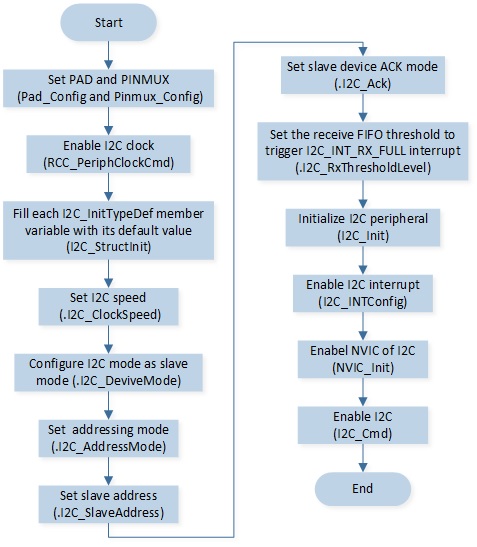
The codes below demonstrate the I2C slave mode initialization flow.
RCC_PeriphClockCmd(APBPeriph_I2C1, APBPeriph_I2C1_CLOCK, ENABLE);

I2C_InitTypeDef  I2C_InitStructure;
I2C_StructInit(&I2C_InitStructure);

I2C_InitStructure.I2C_ClockSpeed = 100000;
I2C_InitStructure.I2C_DeviveMode = I2C_DeviveMode_Slave;
I2C_InitStructure.I2C_AddressMode = I2C_AddressMode_7BIT;
I2C_InitStructure.I2C_SlaveAddress = 0x50;
I2C_InitStructure.I2C_Ack = I2C_Ack_Enable;

I2C_Init(I2C1, &I2C_InitStructure);

/* Config I2C interrupt */
I2C_INTConfig(I2C1, I2C_INT_RD_REQ | I2C_INT_RX_FULL | I2C_INT_STOP_DET, ENABLE);

NVIC_InitTypeDef NVIC_InitStruct;
NVIC_InitStruct.NVIC_IRQChannel = I2C1_IRQn;
NVIC_InitStruct.NVIC_IRQChannelPriority = 3;
NVIC_InitStruct.NVIC_IRQChannelCmd = ENABLE;
NVIC_Init(&NVIC_InitStruct);

I2C_Cmd(I2C1, ENABLE);
Master Write
The codes below demonstrate the operation flow of I2C sending data in master mode.
uint8_t I2C_WriteBuf[16] = {0xaa, 0xbb, 0x66, 0x68, 0x77, 0x88};

if (I2C_Success != I2C_MasterWrite(I2C1, I2C_WriteBuf, 6))
{
    IO_PRINT_ERROR0("i2c_mw_demo: Send failed");

    //Check Event
    if (I2C_CheckEvent(I2C1, ABRT_7B_ADDR_NOACK) == SET)
    {
        IO_PRINT_ERROR0("i2c_mw_demo: Wrong addr");
    }
    if (I2C_CheckEvent(I2C1, ABRT_GCALL_NOACK) == SET)
    {
        IO_PRINT_ERROR0("i2c_mw_demo: General call nack");
    }
    I2C_SendCmd(I2C1, I2C_WRITE_CMD, 0, I2C_STOP_ENABLE);
    I2C_Cmd(I2C1, DISABLE);
    I2C_Cmd(I2C1, ENABLE);
    I2C_MasterWrite(I2C1, I2C_WriteBuf, 6);
}
Master Repeat Read
The codes below demonstrate the operation flow of I2C send and receive data in master mode.
uint8_t I2C_WriteBuf[16] = {0xaa, 0xbb, 0x66, 0x68, 0x77, 0x88};
uint8_t I2C_ReadBuf[16] = {0, 0, 0, 0};

if (I2C_Success != I2C_RepeatRead(I2C1, I2C_WriteBuf, 2, I2C_ReadBuf, 4))
{
    IO_PRINT_ERROR0("i2c_polling_demo: Send failed");

    //Check Event
    if (I2C_CheckEvent(I2C1, ABRT_7B_ADDR_NOACK) == SET)
    {
        IO_PRINT_ERROR0("i2c_polling_demo: Wrong addr");
    }
    if (I2C_CheckEvent(I2C1, ABRT_GCALL_NOACK) == SET)
    {
        IO_PRINT_ERROR0("i2c_polling_demo: General call nack");
    }
}
SPI
SPI Demo Code Support List
Demo 1 |
spi_switchcs_demo.c |
|---|---|
Sample Purpose |
Demonstrate how SPI dynamically switches CS signals. |
File Path |
|
Function Entry |
|
Hardware Connection |
As shown in SPI Demo 1 Hardware Connection Diagram. Connect M1_3 to CS of SPI slave device 0, connect M1_4 to CS of SPI slave device 1, connect M1_5 to CS of SPI slave device 2, connect M1_0 to SCK of SPI slave device 0/1/2, connect M1_1 to MISO of SPI slave device 0/1/2, and connect M1_2 to MOSI of SPI slave device 0/1/2. |
SPI CS0 Pin Definition |
|
SPI CS1 Pin Definition |
|
SPI CS2 Pin Definition |
|
SPI SCK Pin Definition |
|
SPI MOSI Pin Definition |
|
SPI MISO Pin Definition |
|
SPI ID |
SPI1 |
Mode |
Master |
Speed |
400000 |
Data Size |
8-Bit |
Expected Result |
1. Press the reset button on the EVB. The data in array |
Demo 2 |
spi_master_eeprom_mode_demo.c |
|---|---|
Sample Purpose |
Demonstrate how SPI receives data with EEPROM mode by GDMA in master mode. |
File Path |
|
Function Entry |
|
Hardware Connection |
As shown in SPI Demo 2/6 Hardware Connection Diagram. Connect M0_3 to CS of SPI slave device, connect M0_0 to SCK of SPI slave device, connect M0_1 to MISO of SPI slave device, and connect M0_2 to MOSI of SPI slave device. |
SPI CS Pin Definition |
|
SPI SCK Pin Definition |
|
SPI MOSI Pin Definition |
|
SPI MISO Pin Definition |
|
SPI ID |
SPI1 |
Mode |
Master |
Speed |
400000 |
Data Size |
8-Bit |
Expected Result |
Print string ‘spi_master_rx_dma_handler’ and the received data in Debug Analyzer. |
Demo 3 |
external_flash.c |
|---|---|
Sample Purpose |
Demonstrate how the chip communicates with external flash by SPI. |
File Path |
|
Function Entry |
|
Hardware Connection |
As shown in SPI Demo 3 Hardware Connection Diagram. Connect M5_1 to CS of external flash, connect M5_0 to SCK of external flash, connect M5_3 to MISO of external flash, and connect M5_2 to MOSI of external flash, connect M5_5 to HOLD of external flash. |
SPI CS Pin Definition |
|
SPI SCK Pin Definition |
|
SPI MOSI Pin Definition |
|
SPI MISO Pin Definition |
|
FLASH HOLD Pin Definition |
|
SPI ID |
SPI0 |
Mode |
Master |
Speed |
400000 |
Data Size |
8-Bit |
Expected Result |
1. Print string ‘flash_test_task: test_case 1 success’ in Debug Analyzer. |
Demo 4 |
spi_master_demo.c |
|---|---|
Sample Purpose |
Demonstrate how SPI sends data by polling and receives data by interrupt in master mode. |
File Path |
|
Function Entry |
|
Hardware Connection |
As shown in SPI Demo 4 Hardware Connection Diagram. Connect M0_1 to CS of SPI slave device, connect M0_0 to SCK of SPI slave device, connect M1_0 to MISO of SPI slave device, and connect M1_1 to MOSI of SPI slave device. |
SPI CS Pin Definition |
|
SPI SCK Pin Definition |
|
SPI MOSI Pin Definition |
|
SPI MISO Pin Definition |
|
SPI ID |
SPI1 |
Mode |
Master |
Speed |
400000 |
Data Size |
8-Bit |
Expected Result |
1. Press the reset button on the EVB. The data in array |
Demo 5 |
spi_demo.c |
|---|---|
Sample Purpose |
Demonstrate how SPI sends and receives data by polling in master mode. |
File Path |
|
Function Entry |
|
Hardware Connection |
As shown in SPI Demo 5 Hardware Connection Diagram. Connect M1_5 to CS of SPI slave device, connect M1_2 to SCK of SPI slave device, connect M1_3 to MISO of SPI slave device, and connect M1_4 to MOSI of SPI slave device. |
SPI CS Pin Definition |
|
SPI SCK Pin Definition |
|
SPI MOSI Pin Definition |
|
SPI MISO Pin Definition |
|
SPI ID |
SPI1 |
Mode |
Master |
Speed |
400000 |
Data Size |
8-Bit |
Expected Result |
1. Press the reset button on the EVB. The data in array |
Demo 6 |
spi_master_rx_only_mode_demo.c |
|---|---|
Sample Purpose |
Demonstrate how SPI receives data with receive only mode by GDMA in master mode. |
File Path |
|
Function Entry |
|
Hardware Connection |
As shown in SPI Demo 2/6 Hardware Connection Diagram. Connect M0_3 to CS of SPI slave device, connect M0_0 to SCK of SPI slave device, connect M0_1 to MISO of SPI slave device, and connect M0_2 to MOSI of SPI slave device. |
SPI CS Pin Definition |
|
SPI SCK Pin Definition |
|
SPI MOSI Pin Definition |
|
SPI MISO Pin Definition |
|
SPI ID |
SPI1 |
Mode |
Master |
Speed |
400000 |
Data Size |
8-Bit |
Expected Result |
Print string ‘spi_master_rx_dma_handler’ and the received data in Debug Analyzer. |
Demo 7 |
spi_slave_demo.c |
|---|---|
Sample Purpose |
Demonstrate how SPI receives data by interrupt in slave mode. |
File Path |
|
Function Entry |
|
Hardware Connection |
As shown in SPI Demo 7 Hardware Connection Diagram. Connect MIC2_N to CS of SPI master device, connect MIC1_P to SCK of SPI master device, connect MIC2_P to MISO of SPI master device, and connect MIC1_N to MOSI of SPI master device. |
SPI CS Pin Definition |
|
SPI SCK Pin Definition |
|
SPI MOSI Pin Definition |
|
SPI MISO Pin Definition |
|
SPI ID |
SPI0 |
Mode |
Slave |
Data Size |
8-Bit |
Expected Result |
Master device sends data to the chip. The chip stores the received data in array |
Demo 8 |
spi_slave_gpio_demo.c |
|---|---|
Sample Purpose |
Demonstrate how SPI sends data in slave mode by interrupt. |
File Path |
|
Function Entry |
|
Hardware Connection |
As shown in SPI Demo 8 Hardware Connection Diagram. Connect M1_4 to M1_0, connect M1_7 to M1_3, connect M1_5 to M1_2, connect M1_6 to M1_1, and connect M2_3 to M2_4. |
SPI0 CS Pin Definition |
|
SPI0 SCK Pin Definition |
|
SPI0 MOSI Pin Definition |
|
SPI0 MISO Pin Definition |
|
SPI1 CS Pin Definition |
|
SPI1 SCK Pin Definition |
|
SPI1 MOSI Pin Definition |
|
SPI1 MISO Pin Definition |
|
SPI ID |
SPI0 |
Mode |
SPI1 is master, SPI0 is slave. |
Speed |
100000 |
Data Size |
8-Bit |
Expected Result |
1. Master device sends data to slave. The slave stores the received data in array |
Demo 9 |
spi_slave_write_demo.c |
|---|---|
Sample Purpose |
Demonstrate how SPI sends data in slave mode by GDMA. |
File Path |
|
Function Entry |
|
Hardware Connection |
As shown in SPI Demo 9 Hardware Connection Diagram. Connect M2_2 to CS of SPI master device, connect M1_0 to SCK of SPI master device, connect M1_1 to MISO of SPI master device, and connect M2_1 to MOSI of SPI master device. |
SPI CS Pin Definition |
|
SPI SCK Pin Definition |
|
SPI MOSI Pin Definition |
|
SPI MISO Pin Definition |
|
SPI ID |
SPI0 |
Mode |
Slave |
Data Size |
8-Bit |
Expected Result |
1. The data in array sendbuf is sent to SPI master device and prints the string ‘spi_slave_tx_dma_handler’ in Debug Analyzer. |
Demo 10 |
spi0_hs_dma_demo.c |
|---|---|
Sample Purpose |
Demonstrate how SPI0 sends and receives data in high-speed mode. |
File Path |
|
Function Entry |
|
Hardware Connection |
As shown in SPI Demo 10 Hardware Connection Diagram. Connect M1_2 to CS of SPI slave device, connect M1_3 to SCK of SPI slave device, connect M1_4 to MISO of SPI slave device, and connect M1_5 to MOSI of SPI slave device. |
SPI CS Pin Definition |
|
SPI SCK Pin Definition |
|
SPI MOSI Pin Definition |
|
SPI MISO Pin Definition |
|
SPI ID |
SPI0 |
Mode |
Master |
Speed |
40MHz |
Data Size |
8-Bit |
Expected Result |
1. Press the reset button on the EVB and the data in array |
Demo 11 |
spi2spi_auto_reload_dma.c |
|---|---|
Sample Purpose |
Demonstrate how SPI0 reads data and SPI1 sends data by GDMA. |
File Path |
|
Function Entry |
|
Hardware Connection |
As shown in SPI Demo 11/12 Hardware Connection Diagram. Connect M1_7 to CS of SPI slave device 0, connect M1_4 to SCK of SPI slave device 0, connect M1_5 to MISO of SPI slave device 0, and connect M1_6 to MOSI of SPI slave device 0. Connect M2_5 to CS of SPI slave device 1, connect M2_2 to SCK of SPI slave device 1, connect M2_3 to MISO of SPI slave device 1, and connect M2_4 to MOSI of SPI slave device 1. |
SPI0 CS Pin Definition |
|
SPI0 SCK Pin Definition |
|
SPI0 MOSI Pin Definition |
|
SPI0 MISO Pin Definition |
|
SPI1 CS Pin Definition |
|
SPI1 SCK Pin Definition |
|
SPI1 MOSI Pin Definition |
|
SPI1 MISO Pin Definition |
|
SPI ID |
SPI0 |
Mode |
Master |
Speed |
400000 |
Data Size |
8-Bit |
Expected Result |
SPI0 reads data from SPI slave device 0 and SPI1 sends the same data to SPI slave device 1. |
Demo 12 |
spi2spi_dma_demo.c |
|---|---|
Sample Purpose |
Demonstrate how SPI0 reads data and SPI1 sends data by auto-reload GDMA. |
File Path |
|
Function Entry |
|
Hardware Connection |
As shown in SPI Demo 11/12 Hardware Connection Diagram. Connect M1_7 to CS of SPI slave device 0, connect M1_4 to SCK of SPI slave device 0, connect M1_5 to MISO of SPI slave device 0, and connect M1_6 to MOSI of SPI slave device 0. Connect M2_5 to CS of SPI slave device 1, connect M2_2 to SCK of SPI slave device 1, connect M2_3 to MISO of SPI slave device 1, and connect M2_4 to MOSI of SPI slave device 1. |
SPI0 CS Pin Definition |
|
SPI0 SCK Pin Definition |
|
SPI0 MOSI Pin Definition |
|
SPI0 MISO Pin Definition |
|
SPI1 CS Pin Definition |
|
SPI1 SCK Pin Definition |
|
SPI1 MOSI Pin Definition |
|
SPI1 MISO Pin Definition |
|
SPI ID |
SPI0 |
Mode |
Master |
Speed |
400000 |
Data Size |
8-Bit |
Expected Result |
SPI0 reads data from SPI slave device 0 and SPI1 sends the same data to SPI slave device 1. |
Demo 13 |
spi_slave_rx_dma_hs_demo.c |
|---|---|
Sample Purpose |
Demonstrate how SPI0 slave reads data at high speed in GDMA mode. |
File Path |
|
Function Entry |
|
Hardware Connection |
As shown in SPI Demo 13/14 Hardware Connection Diagram. Connect M1_1 to the CS of the SPI master device, connect M0_0 to the SCK of the SPI master device, connect M0_1 to the MISO of the SPI master device, and connect M1_0 to the MOSI of the SPI master device. |
SPI CS Pin Definition |
|
SPI SCK Pin Definition |
|
SPI MOSI Pin Definition |
|
SPI MISO Pin Definition |
|
SPI ID |
SPI0 |
Mode |
Slave |
Speed |
10MHz |
Data Size |
8-Bit |
Expected Result |
Print the string ‘spi_slave_rx_dma_handler! rx_len_all 1000’ and the received data in Debug Analyzer. |
Demo 14 |
spi_slave_tx_dma_hs_demo.c |
|---|---|
Sample Purpose |
Demonstrate how SPI0 slave sends data at high speed in GDMA mode. |
File Path |
|
Function Entry |
|
Hardware Connection |
As shown in SPI Demo 13/14 Hardware Connection Diagram. Connect M1_1 to the CS of the SPI master device, connect M0_0 to the SCK of the SPI master device, connect M0_1 to the MISO of the SPI master device, and connect M1_0 to the MOSI of the SPI master device. |
SPI CS Pin Definition |
|
SPI SCK Pin Definition |
|
SPI MOSI Pin Definition |
|
SPI MISO Pin Definition |
|
SPI ID |
SPI0 |
Mode |
Slave |
Speed |
10MHz |
Data Size |
8-Bit |
Expected Result |
The data in the array |
Demo 15 |
spi_rgb_polling_demo.c |
|---|---|
Sample Purpose |
Demonstrate how SPI1 uses one data line to control the LED in polling mode. |
File Path |
|
Function Entry |
|
Hardware Connection |
Connect M1_0 to the LED controller. |
SPI MOSI Pin Definition |
|
SPI ID |
SPI1 |
Mode |
Master |
Speed |
10MHz |
Data Size |
8-Bit |
Expected Result |
Press the reset button on the EVB, the data in the array |
Demo 16 |
spi_rgb_interrupt_demo.c |
|---|---|
Sample Purpose |
Demonstrate how SPI1 uses one data line to control the LED in interrupt mode. |
File Path |
|
Function Entry |
|
Hardware Connection |
Connect M1_0 to the LED controller. |
SPI MOSI Pin Definition |
|
SPI ID |
SPI1 |
Mode |
Master |
Speed |
10MHz |
Data Size |
8-Bit |
Expected Result |
Press the reset button on the EVB, the data in the array |
Demo 17 |
spi_rgb_dma_demo.c |
|---|---|
Sample Purpose |
Demonstrate how SPI1 uses one data line to control the LED in GDMA mode. |
File Path |
|
Function Entry |
|
Hardware Connection |
Connect M1_0 to the LED controller. |
SPI MOSI Pin Definition |
|
SPI ID |
SPI1 |
Mode |
Master |
Speed |
10MHz |
Data Size |
8-Bit |
Expected Result |
Press the reset button on the EVB, the data in the array |
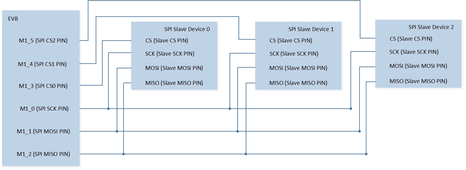
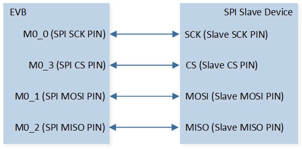
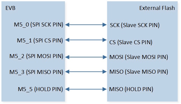
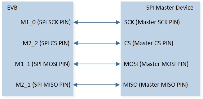

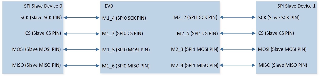

Function Description
SPI allows the chip to communicate with external devices in half/full duplex, synchronous, and serial modes.
Feature List
Support master and slave modes.
Four transfer modes: full-duplex, TX only, RX only, EEPROM.
Support 4-bit to 32-bit data size in master mode.
Support 4-bit to 16-bit data size in slave mode.
Support up to 3 slave devices in master mode.
Support GDMA.
The maximum SPI clock supported by SPI in master mode and slave mode is as follows:
IC Type |
SPI0 Master Max Clock (MHz) |
SPI1 Master Max Clock (MHz) |
SPI2 Master Max Clock (MHz) |
SPI0 Slave Max Clock (MHz) |
|---|---|---|---|---|
RTL87x3E |
50 (with dedicated I/Os) |
20 (with dedicated I/Os) |
20 (with dedicated I/Os) |
10 |
TL87x3EP |
50 (with dedicated I/Os) |
20 (with dedicated I/Os) |
20 (with dedicated I/Os) |
10 |
RTL87x3D |
40 (with dedicated I/Os) |
20 (with dedicated I/Os) |
20 (with dedicated I/Os) |
10 |
Note
RTL87x3D, RTL87x3E, and RTL87x3EP support 3 SPI. SPI0 supports master mode and slave mode. SPI1 and SPI2 only support master mode.
SPI0 and SPI1 support 3 slave devices in master mode, and SPI2 supports 1 slave device in master mode.
If the user needs to operate flash and read data from flash, it is recommended to use SPI_Direction_EEPROM mode. In this mode, the SPI controller will automatically supplement the padding bits needed for reading back. Set the read data length by
SPI_SetReadLen()before reading from flash, then the result ofSPI_GetRxFIFOLen()will equal this value. If SPI_Direction_FullDuplex mode is used when operating flash, it needs to supplement the padding bits manually, and the number of bytes should be equal to the read data length. In this way, the result ofSPI_GetRxFIFOLen()is the total length of padding bits and data to read.SPI_SetReadLen()is just for SPI_Direction_EEPROM mode.SPI support up to 50MHz(SPI0 of RTL87x3E and RTL87x3EP), 40MHz(SPI0 of RTL87x3D) and 20MHz(SPI1 and SPI2) with dedicated I/Os, support 10MHz with general I/Os. For dedicated I/O, please refer to the HDK related documentation.
SPI Communication Sequence Diagram
SPI supports mode 0 to mode 3:
SPI Mode |
Clock Polarity (CPOL) |
Clock Phase (CPHA) |
|---|---|---|
Mode 0 |
0 |
0 |
Mode 1 |
0 |
1 |
Mode 2 |
1 |
0 |
Mode 3 |
1 |
1 |
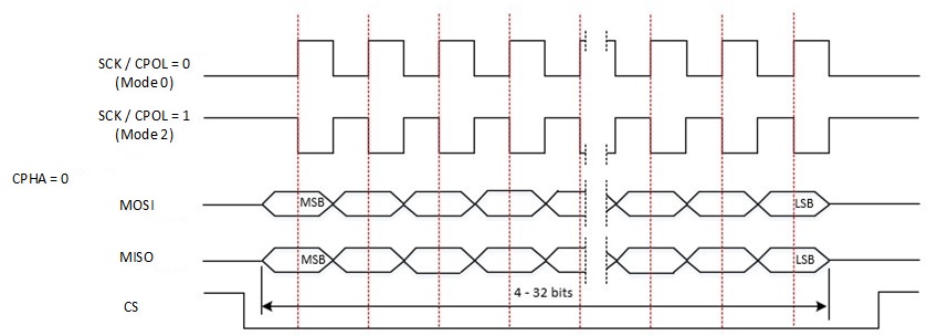
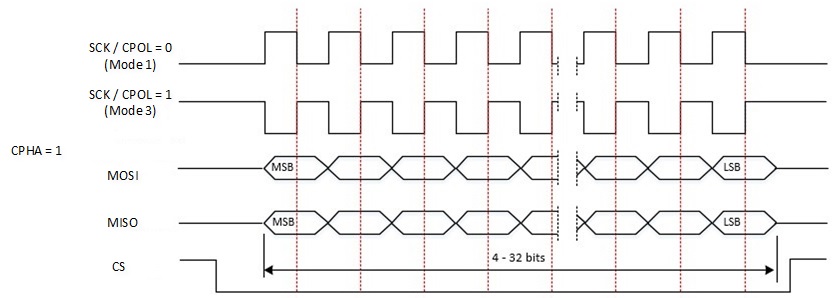
SPI Initialization Flow
SPI initialization flow is shown in the following figure.
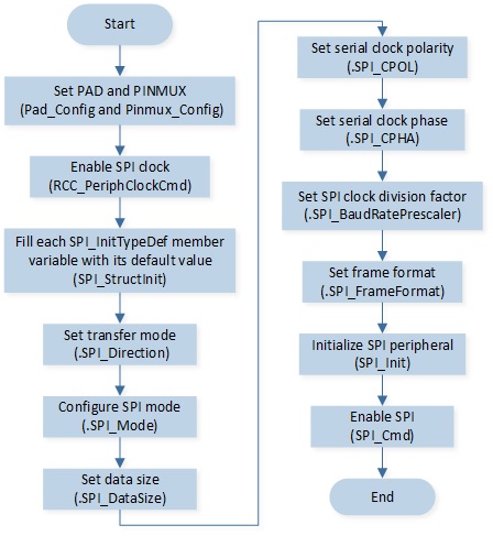
The codes below demonstrate the SPI initialization flow.
void driver_spi_init(void)
{
    /* turn on SPI clock */
    RCC_PeriphClockCmd(APBPeriph_SPI1, APBPeriph_SPI1_CLOCK, ENABLE);

    SPI_InitTypeDef  SPI_InitStructure;
    SPI_StructInit(&SPI_InitStructure);

    SPI_InitStructure.SPI_Direction   = SPI_Direction_FullDuplex;
    SPI_InitStructure.SPI_Mode        = SPI_Mode_Master;
    SPI_InitStructure.SPI_DataSize    = SPI_DataSize_8b;
    SPI_InitStructure.SPI_CPOL        = SPI_CPOL_High;
    SPI_InitStructure.SPI_CPHA        = SPI_CPHA_1Edge;
    SPI_InitStructure.SPI_BaudRatePrescaler  = 100;
    SPI_InitStructure.SPI_FrameFormat = SPI_Frame_Motorola;

    SPI_Init(SPI1, &SPI_InitStructure);
    SPI_Cmd(SPI1, ENABLE);
}
SPI External Flash
This section introduces how to communicate with external flash by SPI. Please refer to SPI Sample Code 3 Description for demo code and refer to SPI Demo 3 Hardware Connection Diagram for hardware connection.
Hardware Connection
Users need to modify the pins related to external flash in the code according to the hardware design. The macro definition below shows the pins defined in the code.
#define FLASH_SCK                   P5_0
#define FLASH_MOSI                  P5_2
#define FLASH_MISO                  P5_3
#define FLASH_CS                    P5_1
#define FLASH_HOLD                  P5_5
Demo Code
Users can implement functions to communicate with external flash by referring to the demo code in SPI Sample Code 3 Description.
Commands for External Flash
Different flash models may have different commands, and users can modify the following definitions according to the flash specifications.
typedef enum
{
    EXT_FLASH_WRITE_STATUS_CMD      = 0x01,
    EXT_FLASH_PROGRAM_CMD           = 0x02,
    EXT_FLASH_READ_CMD              = 0x03,
    EXT_FLASH_WRITE_DISABLE_CMD     = 0x04,
    EXT_FLASH_READ_STATUS_CMD       = 0x05,
    EXT_FLASH_WRITE_ENABLE_CMD      = 0x06,
    EXT_FLASH_SECTOR_ERASE_CMD      = 0x20,
    EXT_FLASH_BLOCK_ERASE_32_CMD    = 0x52,
    EXT_FLASH_CHIP_ERASE_CMD        = 0x60,
    EXT_FLASH_BLOCK_ERASE_64_CMD    = 0xd8,
    EXT_FLASH_READ_ID_CMD           = 0x9F,
    EXT_FLASH_RELEASE_DEEP_SLEEP    = 0xAB,
    EXT_FLASH_DEEP_SLEEP            = 0xB9,
    EXT_FLASH_SOFTWARE_RESET_ENABLE = 0x66,
    EXT_FLASH_SOFTWARE_RESET        = 0x99,
} EXT_FLASH_OPERATION_CMD;
Initialization of External Flash
Users can refer to the following function to initialize external flash. In this function, it will initialize SPI and reset external flash.
void ext_flash_spi_init(void)
Erase External Flash
Users can refer to the following function to erase external flash. Sector, block, and chip are the three common erase commands used for flash.
EXT_FLASH_SPI_OPERATION_STATUS ext_flash_spi_erase(uint32_t address, EXT_FLASH_OPERATION_CMD mode)
Write External Flash
Users can refer to the following function to write external flash by polling mode.
EXT_FLASH_SPI_OPERATION_STATUS ext_flash_spi_page_program(uint32_t address, uint8_t *psendBuf, uint16_t len)
Users can refer to the following function to write external flash by interrupt mode.
EXT_FLASH_SPI_OPERATION_STATUS ext_flash_spi_page_program_by_interrupt(uint32_t address, uint8_t *psendBuf, uint16_t len)
Users can refer to the following function to write external flash by GDMA mode.
EXT_FLASH_SPI_OPERATION_STATUS ext_flash_spi_page_program_by_dma(uint32_t address, uint8_t *psendBuf, uint16_t len)
Read External Flash
Users can refer to the following function to read external flash by polling mode.
EXT_FLASH_SPI_OPERATION_STATUS ext_flash_spi_read(uint32_t address, uint8_t *pStoreBuf, uint16_t len)
Users can refer to the following function to read external flash by interrupt mode.
EXT_FLASH_SPI_OPERATION_STATUS ext_flash_spi_read_by_interrupt(uint32_t address, uint8_t *pStoreBuf, uint16_t len)
Users can refer to the following function to read external flash by GDMA mode.
EXT_FLASH_SPI_OPERATION_STATUS ext_flash_spi_read_by_dma(uint32_t address, uint8_t *pStoreBuf, uint16_t len)
SPI Slave Note
The SPI slave does not support TX FIFO underflow conditions. The TX FIFO needs to be filled with data before the SPI master starts the transfer. There are two methods to avoid this condition:
Send data to the SPI slave TX FIFO before transmission, then toggle a GPIO to notify the SPI master to send data. For the specific implementation, please refer to the demo code in
src\sample\io_demo\spi\slave\spi_slave_gpio_demo.c.Use GDMA for the SPI slave to send data: Enable TX GDMA immediately after SPI slave init to ensure that there is always data in the SPI slave TX FIFO.
Note
If TX FIFO underflow occurs, users can reset SPI slave to recover.
For details, please refer to src\sample\io_demo\spi\slave\spi_slave_tx_dma_hs_demo.c.
SPI GDMA Flow Based on GPIO Indication
This section introduces SPI slave transfers based on GPIO Indication when communicating with the SPI master in GDMA mode. The SPI slave must send data to the TX FIFO before the SPI master starts to communicate with the SPI slave; otherwise, it will trigger TX FIFO underflow error interrupt for the SPI slave. Users can use GPIO to control the timing between the SPI master and the SPI slave. A GPIO pin needs to be toggled for the SPI slave to indicate that the TX data is ready, and the SPI master can transfer data afterward. For the detailed flow, please refer to SPI MISO Flow Chart.
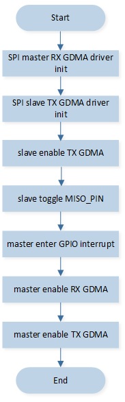
SPI GDMA Note
If SPI is operated in CPU mode with GDMA handshake enabled, it may cause GDMA to get the false signal. So if it’s needed for SPI to read or write by GDMA after CPU mode, the GDMA handshake must be reset before starting GDMA.
SPI_GDMACmd(FLASH_SPI, SPI_GDMAReq_Rx, DISABLE);
SPI_GDMACmd(FLASH_SPI, SPI_GDMAReq_Rx, ENABLE);
GDMA_Cmd(SPI_RX_DMA_CHANNEL_NUM, ENABLE);
SPI Slave High Speed
The SPI slave needs to adjust the slow clock to support high speed, as shown in SPI Slow Clock Settings in RTL87x3E and SPI Slow Clock Settings in RTL87x3D.
For details, please refer to the demo code in src\sample\io_demo\spi\slave\spi_slave_tx_dma_hs_demo.c
and src\sample\io_demo\spi\slave\spi_slave_rx_dma_hs_demo.c.
SPI Clock Div |
SPI Clock |
Slave RX Slow Clock |
Slave TX Slow Clock |
|---|---|---|---|
16 |
2.5MHz |
/ |
1.25MHz |
10 |
4MHz |
/ |
1.25MHz |
8 |
5MHz |
/ |
2.5MHz |
4 |
10MHz |
2.5M |
4MHz |
SPI Clock Div |
SPI Clock |
Slave TX Slow Clock |
|---|---|---|
8 |
5MHz |
2.5MHz |
4 |
10MHz |
5MHz |
IR
IR Demo Code Support List
Demo 1 |
ir_send_polling_mode_demo.c |
|---|---|
Sample Purpose |
Demonstrate how IR sends data by polling mode. |
File Path |
|
Function Entry |
|
Hardware Connection |
Connect M2_2 to channel 0 of the logic analyzer. |
Pin Definition |
|
Expected Result |
The waveform displayed by channel 0 of the logic analyzer is shown in IR Demo 1 Expected Result Diagram. |
Demo 2 |
ir_send_interrupt_demo.c |
|---|---|
Sample Purpose |
Demonstrate how IR sends data by interrupt mode. |
File Path |
|
Function Entry |
|
Hardware Connection |
Connect M2_2 to channel 0 of the logic analyzer. |
Pin Definition |
|
Expected Result |
The waveform displayed by channel 0 of the logic analyzer is shown in IR Demo 2 Expected Result Diagram. |
Demo 3 |
ir_receive_demo.c |
|---|---|
Sample Purpose |
Demonstrate how IR receives data by interrupt mode. |
File Path |
|
Function Entry |
|
Hardware Connection |
Connect M0_2 to the receiving end of the IR transceiver module, connect VCC of EVB to VCC of IR transceiver module, and connect GND of EVB to GND of IR transceiver module. |
Pin Definition |
|
Expected Result |
Send IR data to the IR transceiver module by IR remote control. The received data is stored in array |
Demo 4 |
ir_pulse_detection_demo.c |
|---|---|
Sample Purpose |
Demonstrate the pulse detection of duty and frequency of a PWM with IR. |
File Path |
|
Function Entry |
|
Hardware Connection |
Connect M2_1 to PWM output. |
Pin Definition |
|
Expected Result |
Print PWM frequency, high level count, and low level count information in Debug Analyzer. |
Demo 5 |
ir_nec_protocol.c |
|---|---|
Sample Purpose |
Demonstrates encoding and decoding data by NEC protocol. |
File Path |
|
Function Entry |
|
Expected Result |
Call the API |


Function Description
The infrared module can realize infrared wireless communication with adjacent devices.
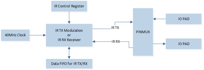
Feature List
Configurable carrier frequency.
Configurable carrier duty cycle.
Configurable carrier ON/OFF time.
Hardware controlled waveform output.
Support any infrared communication protocol.
Support GDMA.
RX mode and TX mode cannot work at the same time.
IR module must be reset when switching between RX mode and TX mode.
IR TX
The schematic diagram of IR TX is shown in the figure below.
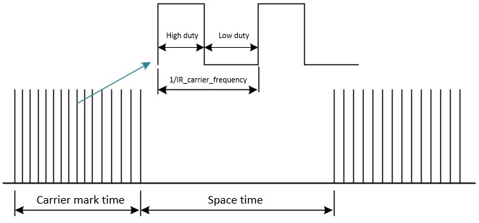
Send Data Operation Flow
IR Initialization Flow
IR initialization flow is shown in the following figure.
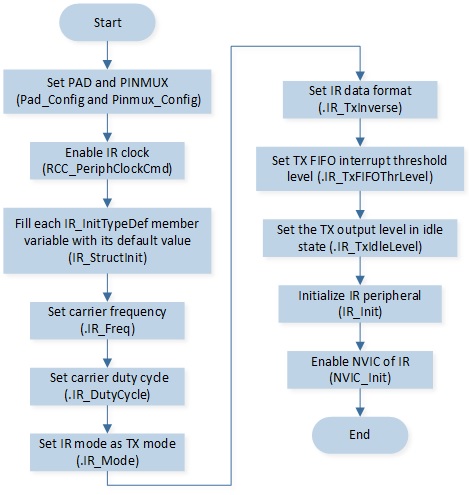
The codes below demonstrate the IR initialization flow.
/* Enable IR clock */
RCC_PeriphClockCmd(APBPeriph_IR, APBPeriph_IR_CLOCK, ENABLE);

/* Initialize IR */
IR_InitTypeDef IR_InitStruct;
IR_StructInit(&IR_InitStruct);
IR_InitStruct.IR_Freq           = 38;
IR_InitStruct.IR_DutyCycle      = 2; /* !< 1/2 duty cycle */
IR_InitStruct.IR_Mode           = IR_MODE_TX;
IR_InitStruct.IR_TxInverse      = IR_TX_DATA_NORMAL;
IR_InitStruct.IR_TxIdleLevel    = IR_IDLE_OUTPUT_LOW;
IR_InitStruct.IR_TxFIFOThrLevel = IR_TX_FIFO_THR_LEVEL;
IR_Init(&IR_InitStruct);

/* Configure NVIC */
NVIC_InitTypeDef NVIC_InitStruct;
NVIC_InitStruct.NVIC_IRQChannel = IR_IRQn;
NVIC_InitStruct.NVIC_IRQChannelPriority = 2;
NVIC_InitStruct.NVIC_IRQChannelCmd = ENABLE;
NVIC_Init(&NVIC_InitStruct);
IR Send Data Operation Flow
IR send data operation flow is shown in the following figure.
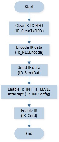
The codes below demonstrate the IR send data operation flow.
/* Buffer which stores encoded data */
IR_DataTypeDef IR_DataStruct;
/* Number of data which has been sent */
uint8_t tx_count = 0;

/* Data to send */
uint8_t ir_code[2] = {0x16, 0x28};

/* Make sure TX FIFO is empty */
IR_ClearTxFIFO();

/* Encode by NEC protocol */
IR_NECEncode(38, ir_code[0], ir_code[1], &IR_DataStruct);

/* Start to send the first bytes of encoded data */
IR_SendBuf(IR_DataStruct.irBuf, IR_TX_FIFO_SIZE, DISABLE);

/* Record the number which has been sent */
tx_count = IR_TX_FIFO_SIZE;

/* Enable IR threshold interrupt. When TX FIFO offset <= threshold value, trigger interrupt*/
IR_INTConfig(IR_INT_TF_LEVEL, ENABLE);

/* Must fill TX FIFO first */
IR_Cmd(IR_MODE_TX, ENABLE);
IR Interrupt Handle Flow
IR interrupt handle flow is shown in the following figure.
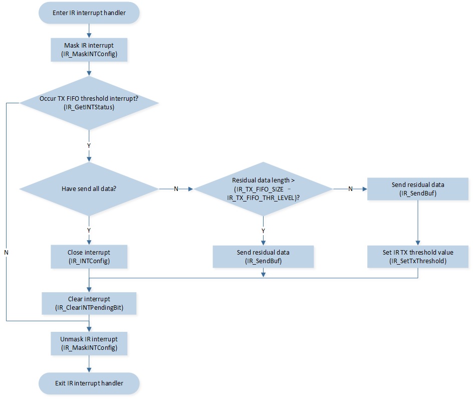
The codes below demonstrate the IR interrupt handle flow.
void ir_handler(void)
{
    /* Continue to send by interrupt */
    if (IR_GetINTStatus(IR_INT_TF_LEVEL) == SET)
    {
        IR_MaskINTConfig(IR_INT_TF_LEVEL, ENABLE);
        /* The remaining data is larger than the TX FIFO length */
        if ((NEC_LENGTH - tx_count) >= IR_TX_FIFO_SIZE)
        {
            IR_SendBuf(IR_DataStruct.irBuf + tx_count, (IR_TX_FIFO_SIZE - IR_TX_FIFO_THR_LEVEL), DISABLE);
            tx_count += (IR_TX_FIFO_SIZE - IR_TX_FIFO_THR_LEVEL);
        }
        else if ((NEC_LENGTH - tx_count) > 0)
        {
            /* The remaining data is less than the TX FIFO length */

            /*  Configure TX threshold level to zero and trigger interrupt when TX FIFO is empty */
            IR_SetTxThreshold(0);
            IR_SendBuf(IR_DataStruct.irBuf + tx_count, NEC_LENGTH - tx_count, ENABLE);
            tx_count += (NEC_LENGTH - tx_count);
        }
        else
        {
            /* Tx completed */
            uint8_t event = IO_DEMO_EVENT_IR_TX;
            /* Disable IR tx empty interrupt */
            IR_INTConfig(IR_INT_TF_LEVEL, DISABLE);
            tx_count = 0;
            if (os_msg_send(io_queue_handle, &event, 0) == false)
            {
                IO_PRINT_ERROR0("ir_handler: Send queue error");
            }
        }

        /* Clear threshold interrupt */
        IR_ClearINTPendingBit(IR_INT_TF_LEVEL_CLR);
        /* Unmask IR interrupt */
        IR_MaskINTConfig(IR_INT_TF_LEVEL, DISABLE);
    }
}
Receive Data Operation Flow
IR Initialization Flow
IR initialization flow is shown in the following figure.
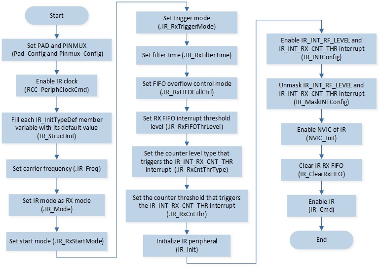
The codes below demonstrate the IR initialization operation flow.
/* Enable IR clock */
RCC_PeriphClockCmd(APBPeriph_IR, APBPeriph_IR_CLOCK, ENABLE);

/* Initialize IR */
IR_InitTypeDef IR_InitStruct;
IR_StructInit(&IR_InitStruct);

IR_InitStruct.IR_Freq               = 38;/* IR carrier frequency is 38KHz */
IR_InitStruct.IR_DutyCycle          = 2;/* Duty ratio = 1/IR_DutyCycle */
IR_InitStruct.IR_Mode               = IR_MODE_RX;/* IR receiving mode */
IR_InitStruct.IR_RxStartMode        = IR_RX_AUTO_MODE;
IR_InitStruct.IR_RxFIFOThrLevel     = IR_RX_FIFO_THR_LEVEL; /* Configure RX FIFO threshold level to trigger IR_INT_RF_LEVEL interrupt */
IR_InitStruct.IR_RxFIFOFullCtrl     = IR_RX_FIFO_FULL_DISCARD_NEWEST;/* Discard the latest received data if RX FIFO is full */
IR_InitStruct.IR_RxTriggerMode      = IR_RX_RISING_EDGE;/* Configure trigger type */
IR_InitStruct.IR_RxFilterTime       = IR_RX_FILTER_TIME_50ns;/* If high to low or low to high transition time <= 50ns, filter it out. */
IR_InitStruct.IR_RxCntThrType       = IR_RX_Count_Low_Level;/* IR_RX_Count_Low_Level is counting low level */
IR_InitStruct.IR_RxCntThr           = 0x23a;/* Configure RX counter threshold. You can use it to decide to stop receiving IR data */
IR_Init(&IR_InitStruct);

/* Enable IR threshold interrupt. When RX FIFO offset >= threshold value, trigger interrupt*/
/* Enable IR counter threshold interrupt to stop receiving data */
IR_INTConfig(IR_INT_RF_LEVEL | IR_INT_RX_CNT_THR, ENABLE);
IR_MaskINTConfig(IR_INT_RF_LEVEL | IR_INT_RX_CNT_THR, DISABLE);

/* Configure NVIC */
NVIC_InitTypeDef NVIC_InitStruct;
NVIC_InitStruct.NVIC_IRQChannel = IR_IRQn;
NVIC_InitStruct.NVIC_IRQChannelPriority = 2;
NVIC_InitStruct.NVIC_IRQChannelCmd = ENABLE;
NVIC_Init(&NVIC_InitStruct);

IR_ClearRxFIFO();
IR_Cmd(IR_MODE_RX, ENABLE);
IR Receive Data Operation Flow
IR receive data operation flow is shown in the following figure.
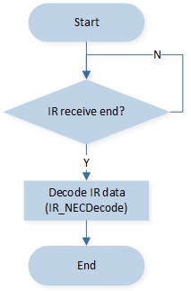
The codes below demonstrate the IR receive data operation flow.
/* Wait for receiving the whole IR packets */
/* This is just a demo. You can send message from IR interrupt handler */
while (rx_count <= NEC_LENGTH - 5) {;};

if (IR_SUCCEED != IR_NECDecode(38, &address, &cmd, &IR_DataStruct))
{
    // Decoding error!
}
else
{
    // Decoding success!
}
IR Interrupt Handle Flow
IR interrupt handle flow is shown in the following figure.
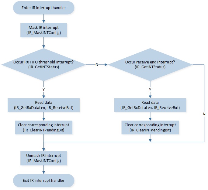
The codes below demonstrate the IR interrupt handle flow.
void ir_handler(void)
{
    uint16_t len = 0;

    /* Receive by interrupt */
    if (IR_GetINTStatus(IR_INT_RF_LEVEL) == SET)
    {
        IR_MaskINTConfig(IR_INT_RF_LEVEL, ENABLE);
        len = IR_GetRxDataLen();
        IR_ReceiveBuf(IR_DataStruct.irBuf + rx_count, len);
        IR_DataStruct.bufLen += len;
        rx_count += len;
        IR_ClearINTPendingBit(IR_INT_RF_LEVEL_CLR);
        IR_MaskINTConfig(IR_INT_RF_LEVEL, DISABLE);
    }

    /* Stop to receive IR data */
    if (IR_GetINTStatus(IR_INT_RX_CNT_THR) == SET)
    {
        IR_MaskINTConfig(IR_INT_RX_CNT_THR, ENABLE);
        /* Read remaining data */
        len = IR_GetRxDataLen();
        IR_ReceiveBuf(IR_DataStruct.irBuf + rx_count, len);
        IR_DataStruct.bufLen += len;
        rx_count += len;
        IR_ClearINTPendingBit(IR_INT_RX_CNT_THR_CLR);
        IR_MaskINTConfig(IR_INT_RX_CNT_THR, DISABLE);
    }
}
RTC
RTC Demo Code Support List
Demo 1 |
rtc_demo.c |
|---|---|
Sample Purpose |
Demonstrate RTC comparator function. |
File Path |
|
Function Entry |
|
Expected Result |
Print string ‘rtc_handler’ in Debug Analyzer every 1536ms. |
Demo 2 |
rtc_overflow_demo.c |
|---|---|
Sample Purpose |
Demonstrate RTC count overflow function. |
File Path |
|
Function Entry |
|
Expected Result |
For RTL87x3D, |
Demo 3 |
rtc_tick_demo.c |
|---|---|
Sample Purpose |
Demonstrate RTC tick function. |
File Path |
|
Function Entry |
|
Expected Result |
|
Demo 4 |
rtc_clock_demo.c |
|---|---|
Sample Purpose |
Demonstrate RTC calendar functionality. |
File Path |
|
Function Entry |
|
Expected Result |
1. Press the reset button on the EVB, string ‘rtc_clock_sys_update: year 2022, month 9, day 29, hour 0, minute 1, second 0’ will be printed in Debug Analyzer. |
Demo 5 |
rtc_in_power_down_mode.c |
|---|---|
Sample Purpose |
Demonstrate RTC work in power down mode. |
File Path |
|
Function Entry |
|
Expected Result |
1. When system is in idle state, it will enter power down mode automatically and print string ‘app_dlps_enter_callback: 10 sec’ in Debug Analyzer. |
Function Description
RTC is an independent timer. RTC has a set of continuous counting counters to provide a calendar clock. It can be converted into the current time and date of the system by querying the counter value.
Feature List
32KHz clock source.
24-bit read-only counter (RTL87x3E and RTL87x3EP), 32-bit read-only counter (RTL87x3D).
12-bit prescaler.
Support 4 comparator interrupts.
Support overflow interrupt, indicating that the counter overflows and wraps around to 0.
Support tick interrupt.
Support wake-up system from low power mode.
Support 8 comparators.
4 comparators can only be used to trigger wake-up.
4 comparators can be used to trigger wake-up and CPU NVIC.
Comparator Function Operation Flow
RTC comparator function initialization flow is shown in the following figure.
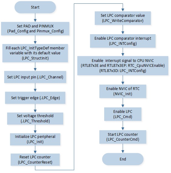
The codes below demonstrate the RTC comparator function initialization flow.
void driver_rtc_init(void)
{
    RTC_DeInit();
    RTC_SetPrescaler(RTC_PRESCALER_VALUE);
    RTC_SetComp(RTC_COMP_INDEX, RTC_COMP_VALUE);
    RTC_MaskINTConfig(RTC_INT_CMP_1, DISABLE);
    RTC_CompINTConfig(RTC_INT_CMP_1, ENABLE);
    RamVectorTableUpdate(RTC_VECTORn, RTC_Handler);

    /* Configure RTC interrupt */
    NVIC_InitTypeDef NVIC_InitStruct;
    NVIC_InitStruct.NVIC_IRQChannel = RTC_IRQn;
    NVIC_InitStruct.NVIC_IRQChannelPriority = 3;
    NVIC_InitStruct.NVIC_IRQChannelCmd = ENABLE;
    NVIC_Init(&NVIC_InitStruct);

    /* Start RTC */
    RTC_SystemWakeupConfig(ENABLE);
    RTC_RunCmd(ENABLE);
}
RTC interrupt handle flow is shown in the following figure.
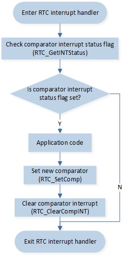
The codes below demonstrate the RTC interrupt handle flow.
void rtc_handler(void)
{
    IO_PRINT_TRACE0("rtc_handler");
    if (RTC_GetINTStatus(RTC_INT_CMP_1) == SET)
    {
        RTC_SetComp(RTC_COMP_INDEX, RTC_GetCounter() + RTC_COMP_VALUE);
        RTC_ClearCompINT(RTC_COMP_INDEX);
    }
}
Overflow Function Operation Flow
RTC overflow function initialization flow is shown in the following figure.
The codes below demonstrate the RTC overflow function initialization flow.
void driver_rtc_init(void)
{
    RTC_DeInit();
    RTC_SetPrescaler(RTC_PRESCALER_VALUE);
    RTC_MaskINTConfig(RTC_INT_OVF, DISABLE);

    RamVectorTableUpdate(RTC_VECTORn, rtc_handler);

    /* Config RTC interrupt */
    NVIC_InitTypeDef NVIC_InitStruct;
    NVIC_InitStruct.NVIC_IRQChannel = RTC_IRQn;
    NVIC_InitStruct.NVIC_IRQChannelPriority = 2;
    NVIC_InitStruct.NVIC_IRQChannelCmd = ENABLE;
    NVIC_Init(&NVIC_InitStruct);

    /* Start RTC */
    RTC_RunCmd(ENABLE);
}
RTC interrupt handle flow is shown in the following figure.
The codes below demonstrate the RTC interrupt handle flow.
void rtc_handler(void)
{
    /* RTC overflow interrupt handle */
    if (RTC_GetINTStatus(RTC_INT_OVF) == SET)
    {
        // Add application code here

        RTC_ClearOverFlowINT();
    }
}
Tick Function Operation Flow
RTC tick function initialization flow is shown in the following figure.
The codes below demonstrate the RTC tick function initialization flow.
void driver_rtc_init(void)
{
    RTC_DeInit();
    RTC_SetPrescaler(RTC_PRESCALER_VALUE);
    RTC_MaskINTConfig(RTC_INT_TICK, DISABLE);
    RTC_TickINTConfig(ENABLE);

    RamVectorTableUpdate(RTC_VECTORn, rtc_handler);

    /* Config RTC interrupt */
    NVIC_InitTypeDef NVIC_InitStruct;
    NVIC_InitStruct.NVIC_IRQChannel = RTC_IRQn;
    NVIC_InitStruct.NVIC_IRQChannelPriority = 2;
    NVIC_InitStruct.NVIC_IRQChannelCmd = ENABLE;
    NVIC_Init(&NVIC_InitStruct);

    /* Start RTC */
    RTC_RunCmd(ENABLE);
}
RTC interrupt handle flow is shown in the following figure.

The codes below demonstrate the RTC interrupt handle flow.
void rtc_handler(void)
{
    /* RTC overflow interrupt handle */
    if (RTC_GetINTStatus(RTC_INT_TICK) == SET)
    {
        // Add application code here

        RTC_ClearTickINT();
    }
}
LPC
LPC Demo Code Support List
Demo 1 |
lpc_comparator_demo.c |
|---|---|
Sample Purpose |
Demonstrate LPC comparator function. |
File Path |
|
Function Entry |
|
Hardware Connection |
Connect M0_0 of EVB to an external DC voltage source. |
Expected Result |
Adjust the DC voltage source repeatedly, when the input voltage on M0_0 is detected to be higher than 400mV for 4 times, the string ‘lpc_rtc_handler: lpc_counter_value 4’ will be printed on Debug Analyzer. |
Demo 2 |
lpc_peri_vol_demo.c |
|---|---|
Sample Purpose |
Demonstrate LPC voltage detection function. |
File Path |
|
Function Entry |
|
Hardware Connection |
Connect M0_0 of EVB to an external DC voltage source. |
Expected Result |
Adjust the DC voltage source, when the input voltage on M0_0 is detected to be lower than 800mV for 6 times, the string ‘lpc_handler: lpc_counter_value 6’ will be printed on Debug Analyzer. |
Demo 3 |
lpc_rtc_vol_demo.c |
|---|---|
Sample Purpose |
Demonstrate LPC voltage detection function. |
File Path |
|
Function Entry |
|
Hardware Connection |
Connect M0_0 of EVB to an external DC voltage source. |
Expected Result |
Adjust the DC voltage source, when the input voltage on M0_0 is detected to be higher than 1200mV for 5 times, the string ‘lpc_rtc_handler: lpc_counter_value 5’ will be printed on Debug Analyzer. |
Function Description
LPC can be used for voltage detection and counting. When the LPC detects that the input voltage exceeds the set voltage threshold, the system will trigger the interrupt. LPC can be used to count the number of times the input voltage exceeds the set voltage threshold. When the count value exceeds the set value of the comparator, the interrupt will be triggered.
Comparator Function Operation Flow
LPC comparator function initialization flow is shown in the following figure.
The codes below demonstrate the LPC comparator function initialization flow.
void driver_lpc_init(void)
{
    LPC_InitTypeDef LPC_InitStruct;
    LPC_StructInit(&LPC_InitStruct);
    LPC_InitStruct.LPC_Channel   = LPC_CAPTURE_PIN;
    LPC_InitStruct.LPC_Edge      = LPC_Vin_Over_Vth;
    LPC_InitStruct.LPC_Threshold = LPC_400_mV;
    LPC_Init(&LPC_InitStruct);

    LPC_CounterReset();
    LPC_WriteComparator(LPC_COMP_VALUE);
    LPC_INTConfig(LPC_INT_COUNT_COMP, ENABLE);

#if (TARGET_RTL87X3E == 1 || CONFIG_SOC_SERIES_RTL8773E == 1)
    RTC_CpuNVICEnable(ENABLE);
    RamVectorTableUpdate(RTC_VECTORn, lpc_rtc_handler);
    /* Config LPC interrupt */
    NVIC_InitTypeDef NVIC_InitStruct;
    NVIC_InitStruct.NVIC_IRQChannel = RTC_IRQn;
    NVIC_InitStruct.NVIC_IRQChannelPriority = 3;
    NVIC_InitStruct.NVIC_IRQChannelCmd = ENABLE;
    NVIC_Init(&NVIC_InitStruct);
#else
    LPC_INTConfig(LPC_INT_VOLTAGE_COMP, ENABLE);
    RamVectorTableUpdate(LPCOMP_VECTORn, lpc_rtc_handler);
    /* Config LPC interrupt */
    NVIC_InitTypeDef NVIC_InitStruct;
    NVIC_InitStruct.NVIC_IRQChannel = LPCOMP_IRQn;
    NVIC_InitStruct.NVIC_IRQChannelPriority = 3;
    NVIC_InitStruct.NVIC_IRQChannelCmd = ENABLE;
    NVIC_Init(&NVIC_InitStruct);
#endif

    LPC_Cmd(ENABLE);
    LPC_CounterCmd(ENABLE);
}
LPC comparator function interrupt handle flow is shown in the figure below.

The codes below demonstrate the LPC comparator function interrupt handle flow.
void lpc_rtc_handler(void)
{
    uint16_t lpc_counter_value = 0;

    IO_PRINT_INFO0("lpc_rtc_handler");

    /* LPC counter comparator interrupt */
    if (LPC_GetINTStatus(LPC_INT_COUNT_COMP) == SET)
    {
        lpc_counter_value = LPC_ReadCounter();
        IO_PRINT_INFO1("lpc_rtc_handler: lpc_counter_value %d", lpc_counter_value);

        LPC_WriteComparator(lpc_counter_value + LPC_COMP_VALUE);
        LPC_ClearINTPendingBit(LPC_INT_COUNT_COMP);
    }
}
Voltage Detection Function Operation Flow
The codes below demonstrate the LPC voltage detection function initialization flow.
void driver_lpc_init(void)
{
    LPC_InitTypeDef LPC_InitStruct;
    LPC_StructInit(&LPC_InitStruct);
    LPC_InitStruct.LPC_Channel   = LPC_CAPTURE_PIN;
    LPC_InitStruct.LPC_Edge      = LPC_Vin_Below_Vth;
    LPC_InitStruct.LPC_Threshold = LPC_800_mV;
    LPC_Init(&LPC_InitStruct);

    LPC_CounterReset();
    LPC_WriteComparator(LPC_COMP_VALUE);
    LPC_INTConfig(LPC_INT_COUNT_COMP, ENABLE);

#if (TARGET_RTL87X3E == 1 || CONFIG_SOC_SERIES_RTL8773E == 1)
    RTC_CpuNVICEnable(ENABLE);
    RamVectorTableUpdate(RTC_VECTORn, lpc_handler);
    /* Config LPC interrupt */
    NVIC_InitTypeDef NVIC_InitStruct;
    NVIC_InitStruct.NVIC_IRQChannel = RTC_IRQn;
    NVIC_InitStruct.NVIC_IRQChannelPriority = 3;
    NVIC_InitStruct.NVIC_IRQChannelCmd = ENABLE;
    NVIC_Init(&NVIC_InitStruct);
#else
    LPC_INTConfig(LPC_INT_VOLTAGE_COMP, ENABLE);
    RamVectorTableUpdate(LPCOMP_VECTORn, lpc_handler);
    /* Config LPC interrupt */
    NVIC_InitTypeDef NVIC_InitStruct;
    NVIC_InitStruct.NVIC_IRQChannel = LPCOMP_IRQn;
    NVIC_InitStruct.NVIC_IRQChannelPriority = 3;
    NVIC_InitStruct.NVIC_IRQChannelCmd = ENABLE;
    NVIC_Init(&NVIC_InitStruct);
#endif

    LPC_Cmd(ENABLE);
    LPC_CounterCmd(ENABLE);
}
The codes below demonstrate the LPC voltage detection function interrupt handle flow.
void lpc_handler(void)
{
    if (LPC_GetINTStatus(LPC_INT_COUNT_COMP) == SET)
    {
        IO_PRINT_INFO1("lpc_handler: lpc_counter_value %d", LPC_ReadCounter());
        LPC_CounterReset();
        LPC_ClearINTPendingBit(LPC_INT_COUNT_COMP);//Add Application code here
        //Add Application code here
    }
}
3-Wire SPI
3-Wire SPI Demo Code Support List
Demo 1 |
spi3wire_demo.c |
|---|---|
Sample Purpose |
Demonstrate how 3-wire SPI single write and read data. |
Brief Introduction |
Use 3-wire SPI for data transmission with PMW3610DM-SUDU mouse sensor. Obtain PMW3610DM-SUDU ID, check whether ID is correct, and print corresponding information in Debug Analyzer. |
File Path |
|
Function Entry |
|
CS Pin Definition |
|
DIO Pin Definition |
|
SCLK Pin Definition |
|
Speed |
800KHz |
Read Delay Time |
2.5us |
Hardware Connection |
As shown in 3-Wire SPI Demo Hardware Connection Diagram. Connect M0_0 of EVB to SCLK of sensor, connect M0_1 of EVB to SDIO of sensor, connect M0_2 of EVB to NCS of sensor, connect GND of EVB to GND of sensor, connect U_5V_FT of EVB to 5V of sensor. |
Expected Result |
Press the reset button on the EVB, if the data transmission is successful, the string ‘spi3wire_demo: Read mouse sensor ID success’ will be printed in Debug Analyzer; otherwise, the string ‘spi3wire_demo: Read mouse sensor ID error’ will be printed in Debug Analyzer. |
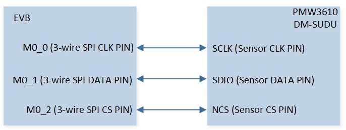
Function Description
3-Wire SPI is used to connect 3-wire SPI interfaces such as CS/DIO/SCLK and has single wire, single/burst read function. It is also possible to adjust the desired delay timing between read/write.
Note
Only RTL87x3D supports 3-wire SPI.
Feature List
Support 2-wire and 3-wire communication.
Support single write and read.
Support burst read.
Configurable delay between write and read.
3-Wire SPI Data Format
The data contains two bytes, the first byte is the address bit, the highest bit is the read/write control bit, and the second byte is the data byte. As shown below:
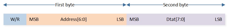
3-Wire SPI Write Operation
Write data from the controller to the sensor, only supports single write mode, as shown in the figure below. No delay needs to be added between the address byte and the data byte.

3-Wire SPI Read Operation
Single Read Mode
Between the first byte (address byte) and the second byte (data byte), a delay of ‘T-hold’ needs to be added. This delay is configured by SPI3WIRE_ReadDelay.

Burst Read Mode
In burst read mode, SPI can continuously read multiple bytes of data. Between the first byte (address byte) and the second byte (data byte 0), a delay of ‘T-hold’ needs to be added. This delay is configured by SPI3WIRE_ReadDelay. There is no delay between the third byte (data byte 1) and the second byte (data byte 0) until the end of a burst read.
Initialization Operation Flow
3-Wire SPI initialization flow is shown in the following figure.
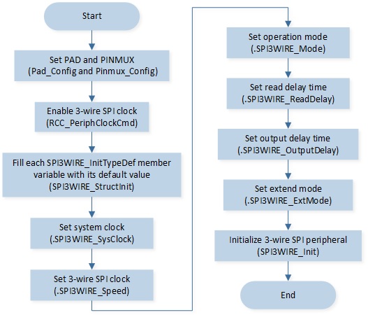
The codes below demonstrate the 3-wire SPI initialization flow.
/* Enable 3-wire SPI clock */
RCC_PeriphClockCmd(APBPeriph_SPI2W, APBPeriph_SPI2W_CLOCK, ENABLE);

/* Initialize 3-wire SPI */
SPI3WIRE_InitTypeDef SPI3WIRE_InitStruct;
SPI3WIRE_StructInit(&SPI3WIRE_InitStruct);

SPI3WIRE_InitStruct.SPI3WIRE_SysClock       = 20000000;
SPI3WIRE_InitStruct.SPI3WIRE_Speed          = 800000;
SPI3WIRE_InitStruct.SPI3WIRE_Mode           = SPI3WIRE_3WIRE_MODE;
/* delay time = (SPI3WIRE_ReadDelay +1)/(2*SPI3WIRE_Speed). The delay time from the end of address phase to the start of read data phase */
//delay time = (0x03 + 1)/(2 * speed) = 2.5us
SPI3WIRE_InitStruct.SPI3WIRE_ReadDelay      = 0x3;
SPI3WIRE_InitStruct.SPI3WIRE_OutputDelay    = SPI3WIRE_OE_DELAY_NONE;
SPI3WIRE_InitStruct.SPI3WIRE_ExtMode        = SPI3WIRE_NORMAL_MODE;
SPI3WIRE_Init(&SPI3WIRE_InitStruct);
Send Data Operation Flow
3-Wire SPI sends data operation flow is shown in the following figure.
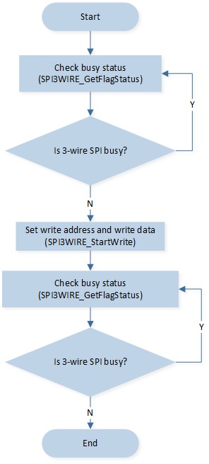
The codes below demonstrate the 3-wire SPI send data operation flow.
bool Mouse_SingleWrite(uint8_t address, uint8_t data)
{
    uint32_t timeout = 0;

    /* Check SPI busy or not */
    while (SPI3WIRE_GetFlagStatus(SPI3WIRE_FLAG_BUSY) == SET)
    {
        timeout++;
        if (timeout > 0x1ffff)
        {
            return false;
        }
    }

    /* Write data */
    SPI3WIRE_StartWrite(address, data);

    timeout = 0;
    /* Wait for communication to end */
    while (SPI3WIRE_GetFlagStatus(SPI3WIRE_FLAG_BUSY) == SET)
    {
        timeout++;
        if (timeout > 0x1ffff)
        {
            return false;
        }
    }
    return true;
}
Receive Data Operation Flow
3-Wire SPI receives data operation flow is shown in the following figure.
The codes below demonstrate the 3-wire SPI receives data operation flow.
uint8_t Mouse_SingleRead(uint8_t address)
{
uint8_t reg_value = 0;
uint32_t timeout = 0;
/* Check SPI busy or not */
while (SPI3WIRE_GetFlagStatus(SPI3WIRE_FLAG_BUSY) == SET)
{
timeout++;
if (timeout > 0x1ffff)
{
break;
}
}
/* Clear Receive data length */
SPI3WIRE_ClearRxDataLen();
SPI3WIRE_StartRead(address, 1);
timeout = 0;
/* Wait for the end of communication */
while (SPI3WIRE_GetFlagStatus(SPI3WIRE_FLAG_BUSY) == SET)
{
timeout++;
if (timeout > 0x1ffff)
{
break;
}
}
/* Get the length of received data */
while (SPI3WIRE_GetRxDataLen() == 0);
/* Read data */
SPI3WIRE_ReadBuf(®_value, 1);
return reg_value;
}
CapTouch
CapTouch Demo Code Support List
Demo 1 |
cap_touch_demo.c |
|---|---|
Sample Purpose |
Demonstrates CapTouch how to detect finger touch and proximity by interrupt. |
Brief Introduction |
This sample code demonstrates CapTouch’s detection of finger touch and proximity through interrupts. In CapTouch interrupt handler, 4 channels can be detected, whether there is finger press/release/false touch/over noise threshold. |
File Path |
|
Function Entry |
|
Channel pin location |
Channel 0: P0_0 |
Expected Result |
Press the reset button on the EVB. When the channel pin is pressed/released, the interrupt status will be printed in Debug Analyzer. |
Function Description
Capacitive touch controller uses a single pin and measures the capacitance between the capacitive sensor pin and ground. Capacitive touch controller uses changes in capacitance to detect the presence of a finger on or near a touch surface.

The sensor parasitic capacitance is called CP. When fingers touch or approach the sensor’s surface, it forms a simple parallel plate capacitor with the sensor pad through the overlay. The result is called finger capacitance CF, it increases the measured capacitance CS: CS = CP + CF.
In the initial state, an amount of charge is built-up on an untouched sensor to set the sensor’s reference level, CS=CP. As the finger makes contact with the sensor, it couples with the electric field of the sensor. This results in a drop of that sensor’s charge - since a portion of that charge is drained off through the finger to ground. Further charge transfers (conversions) from that sensor result in a reduced signal level compared to the untouched state.
Capacitive touch controller as CapTouch System shows is implemented by oversampling a high sensitivity ADC which only requires 1-pin per channel. The ADC will capture the voltage of both the reference level (baseline) and the signal level and transform them into digital raw data. If the difference between the reference level and the signal level is greater than the user-determined finger touch threshold, a touch is detected, and at the same time, a touch interrupt will be sent to the MCU to wake up the top system or other operations.
Capacitive touch controller supports up to 4 capacitive sensing inputs, which offers a wide detection range of capacitance, and best-in-class liquid tolerance. With the smart calibration function enabled, all channels’ sensitivity or thresholds could be adjusted individually according to different noise environments. Both of baseline value and the absolute finger touch threshold value will be calibrated automatically to adapt to environmental variation. The capacitive controller offers an adjustable scan period, resulting in lower power consumption.
Note
RTL87x3E supports CapTouch, RTL87x3D and RTL87x3EP don’t support CapTouch.
Feature List
Support 4 capacitive sensor channels.
Support wide parasitic capacitance range for each channel: 5~45pF (5uA sensitivity).
Support both finger touch detection and proximity detection.
Programmable enable/disable for each channel.
Adjustable sensitivity for each channel: 0.25uA~15.75uA.
Adjustable baseline and touch threshold (both difference and absolute value) for each channel.
Support liquid tolerance: guard sensor.
Programmable channel scan mode.
Auto scan mode: hardware automatically scans every enabled channel in sequence.
Automatic environment sensor capacitance tracking and calibration (ETC).
Support interrupt control.
Low power consumption.
CapTouch Channel Pin Location
Channel 0: P0_0
Channel 1: P0_1
Channel 2: P0_2
Channel 3: P0_3
Sample Range
CapTouch sample range is related to channel sensitivity; the more sensitive the channel, the shorter the sample range. The sensitivity parameter is used to increase or decrease the strength of the sensor signal (difference count), which means different counts for the same capacitance change. A higher value of the sensitivity setting (bias current) leads to a stronger signal from the sensors (more difference count for the same capacitance change), and also causes the decrease of the sample range. The typical sample range of CapTouch is 5~45pF when channel sensitivity is 5uA.
Environment Tracking and Calibration (ETC)
Sensor capacitance changes all the time according to environmental variations, such as temperature, moisture, overlay changes, or other slight environmental noise. The ETC module is built for tracking and calibration with environmental variation. The ETC function operates all the time during low power mode. The ETC system tracks the sensor capacitance change by period and updates the baseline and touch threshold based on the ETC automatic update algorithm.
There is no need for an extra scan operation except an active mode scan operation. ETC auto-tunes all the parameters of the ETC module, it works by capturing and comparing the data of the scan operation, and making a decision to update the baseline and absolute threshold or not.
Manual tuning of ETC parameters is also supported to meet different noise environments or special applications.
Touch Judgement Mode (with ETC Function Enable)
After ADC finishes data processing, decision logic will finish the following operations:
Data average operation.
Make subtraction operations of the average sample data and baseline.
Compare difference data with difference threshold.
If the difference data is larger than the difference threshold, touch or proximity is detected.
Auto Scan Mode
Hardware will scan every enabled channel in sequence during one scan period. For example, if channel 2 is disabled, then hardware will scan channel 0->1->3 once each scan period. The auto scan mode flow as Auto Scan Mode Flow Chart shows.
Scan Period
CapTouch scan period consists of active time and sleep time. Both the active time and sleep time can be set individually for different applications. The scan period as Schematic Diagram of Scan Period shows.
Active Time
The active time of CapTouch is defined by ADC scan sample number. CapTouch averages the sample raw data of capture ADC for best accuracy and noise immunity.
Sleep Time
After all of these operations for each channel, the channel enters the sleep period, and another channel begins to scan and process data. After 4 channels of scanning and data processing are finished, capture ADC power is off, and the CapTouch system enters an ultra-low power state until the next cycle of sensor scanning. During the sleep period, all channels are still enabled, and MCU uses clock gating to save power. Each channel could be disabled while a sensor error is detected or in other situations.
Baseline Auto-Initialization
The baseline initial value is 0x0 when CapTouch function enables, CapTouch will initialize baseline value automatically with ETC function and baseline initial function both are enabled. Hardware will set the baseline with average of ADC raw code. After that, hardware will enter normal scan mode (ETC scan and judge operation).
Noise Threshold
The environmental negative noise threshold means the maximum capacitance change of raw data that is still considered an environmental change. CapTouch system supports 2 noise thresholds: positive noise threshold and negative noise threshold for optimal calibration. Both of the two noise thresholds are individually adjustable for each channel.
Environmental noise usually changes slightly and slowly. Most of the noise average data ranges from 0~50, less than 40% * touch threshold even when Bluetooth or other RF transmissions occur beside the CapTouch device. The recommended value of noise threshold is 40% * touch threshold.
Specific operations take place while a signal changes significantly, which is larger than the noise threshold. For example, when a finger touches the sensor surface, glass or plastic overlay causes the difference data (baseline - signal) to be larger than the negative noise threshold. Glass or plastic being removed from the sensor surface or a finger released after CapTouch initiation both cause the difference data (signal - baseline) to be larger than the positive noise threshold. All of these operations are not normal environment noise variations.
CapTouch sends P_ENT interrupt to the host while the difference (signal - baseline) is larger than the positive noise threshold. The host needs to initialize the baseline when P_ENT is detected. CapTouch instructs the ETC module to ignore the ETC update operation automatically when the difference data (baseline - signal) is larger than the negative noise threshold.
Both noise thresholds need tuning for different applications and noise environments.
Fast Mode
To improve response time, the scan period can become smaller after detecting ADC raw data lower than the threshold. The smaller interval makes for a faster response time and higher power consumption.
Channel False Alarm and Release Active Counter
Fs Match Counter
In idle mode, count how many scans meet the threshold condition. When
fs_match_cntmeets the setting, the scan interval changes from slow mode to fast mode. When settingfs_match_cnt= 0, it will always be in slow mode.False Alarm Counter
Counting for false alarms. When
fs_match_cntmeets anddebounce_cntdoesn’t meet, the false alarm counter will count the scans in fast mode. After the false alarm counter meets, it returns to the idle state (slow interval).Release Active Counter
Counting for release active (triggered by the release active event). After the release active event, counting scans in fast mode. After the release active counter meets, it returns to the idle state (slow mode).
Channel Press Counter
False Touch Counter
Counter for false touch. It starts after the debounce counter meets the setting. After the false touch counter triggers, it is forced to return to the idle state to prevent extra power consumption.
Fast Touch Counter
Counting how many scans meet threshold conditions in fast mode. Calculate the press time according to this counter.
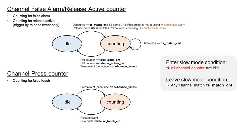
CapTouch Operation Flow
CapTouch initialization flow is shown in the following figure.
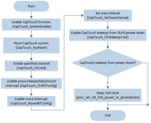
The codes below demonstrate the CapTouch initialization flow.
/* Enable CapTouch function */
CapTouch_SystemEnable(true);

/* Reset CapTouch system and clear all settings */
CapTouch_SysReset();

IO_PRINT_INFO2("cap_touch_demo: Start, max_channel %d, cap_touch_enable %d",
                   CapTouch_GetMaxChannel(), CapTouch_IsSystemEnable());

/* Register new interrupt handler to vector table */
RamVectorTableUpdate(TOUCH_VECTORn, (IRQ_Fun)CapTouch_Handler);

/* Enable specified channel */
CapTouch_ChCmd(CTC_CH0, ENABLE);
CapTouch_ChCmd(CTC_CH1, ENABLE);
CapTouch_ChCmd(CTC_CH2, ENABLE);
CapTouch_ChCmd(CTC_CH3, ENABLE);

/* Enable the specified CapTouch interrupts of specified channel */
CapTouch_ChINTConfig(CTC_CH0, (CTC_CH_INT_TYPE)(CTC_TOUCH_PRESS_INT | CTC_TOUCH_RELEASE_INT |
                                                    CTC_FALSE_TOUCH_INT), ENABLE);
CapTouch_ChINTConfig(CTC_CH1, (CTC_CH_INT_TYPE)(CTC_TOUCH_PRESS_INT | CTC_TOUCH_RELEASE_INT |
                                                    CTC_FALSE_TOUCH_INT), ENABLE);
CapTouch_ChINTConfig(CTC_CH2, (CTC_CH_INT_TYPE)(CTC_TOUCH_PRESS_INT | CTC_TOUCH_RELEASE_INT |
                                                    CTC_FALSE_TOUCH_INT), ENABLE);
CapTouch_ChINTConfig(CTC_CH3, (CTC_CH_INT_TYPE)(CTC_TOUCH_PRESS_INT | CTC_TOUCH_RELEASE_INT |
                                                    CTC_FALSE_TOUCH_INT), ENABLE);

/* Enable the specified CapTouch noise interrupts */
CapTouch_NoiseINTConfig(CTC_OVER_P_NOISE_INT, ENABLE);

/* Set scan interval */
if (!CapTouch_SetScanInterval(0x3B, CTC_SLOW_MODE))
{
    IO_PRINT_WARN0("cap_touch_demo: Slow mode scan interval overrange");
}
if (!CapTouch_SetScanInterval(0x1D, CTC_FAST_MODE))
{
    IO_PRINT_WARN0("cap_touch_demo: Fast mode scan interval overrange");
}

/* Enable touch wakeup from DLPS, PowerDown */
CapTouch_ChWakeupCmd(CTC_CH0, (FunctionalState)ENABLE);
CapTouch_ChWakeupCmd(CTC_CH1, (FunctionalState)ENABLE);
CapTouch_ChWakeupCmd(CTC_CH2, (FunctionalState)ENABLE);
CapTouch_ChWakeupCmd(CTC_CH3, (FunctionalState)ENABLE);

/*Should keep 32k clk if enable wakeup from power down mode*/
pmu_set_clk_32k_power_in_powerdown(true);

/* CapTouch start after 3s later */
CapTouch_Cmd(ENABLE, ENABLE);
CapTouch interrupt handle flow is shown in the following figure.
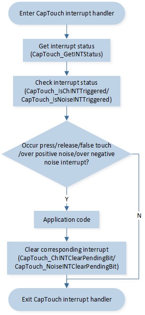
The codes below demonstrate the CapTouch interrupt handle flow.
void captouch_handler(void)
{
    uint32_t int_status = 0;
    int_status = CapTouch_GetINTStatus();
    IO_PRINT_INFO1("captouch_handler: int_status 0x%x", int_status);
    /* Channel 0 interrupts */
    if (CapTouch_IsChINTTriggered(int_status, CTC_CH0, CTC_TOUCH_PRESS_INT))
    {
        /* do something */
        CapTouch_ChINTClearPendingBit(CTC_CH0, CTC_TOUCH_PRESS_INT);
    }
    if (CapTouch_IsChINTTriggered(int_status, CTC_CH0, CTC_TOUCH_RELEASE_INT))
    {
        /* do something */
        CapTouch_ChINTClearPendingBit(CTC_CH0, CTC_TOUCH_RELEASE_INT);
    }
    if (CapTouch_IsChINTTriggered(int_status, CTC_CH0, CTC_FALSE_TOUCH_INT))
    {
        /* do something */
        CapTouch_ChINTClearPendingBit(CTC_CH0, CTC_FALSE_TOUCH_INT);
    }
    /* Channel 1 interrupts */
    if (CapTouch_IsChINTTriggered(int_status, CTC_CH1, CTC_TOUCH_PRESS_INT))
    {
        /* do something */
        CapTouch_ChINTClearPendingBit(CTC_CH1, CTC_TOUCH_PRESS_INT);
    }
    if (CapTouch_IsChINTTriggered(int_status, CTC_CH1, CTC_TOUCH_RELEASE_INT))
    {
        /* do something */
        CapTouch_ChINTClearPendingBit(CTC_CH1, CTC_TOUCH_RELEASE_INT);
    }
    if (CapTouch_IsChINTTriggered(int_status, CTC_CH1, CTC_FALSE_TOUCH_INT))
    {
        /* do something */
        CapTouch_ChINTClearPendingBit(CTC_CH1, CTC_FALSE_TOUCH_INT);
    }
    /* Channel 2 interrupts */
    if (CapTouch_IsChINTTriggered(int_status, CTC_CH2, CTC_TOUCH_PRESS_INT))
    {
        /* do something */
        CapTouch_ChINTClearPendingBit(CTC_CH2, CTC_TOUCH_PRESS_INT);
    }
    if (CapTouch_IsChINTTriggered(int_status, CTC_CH2, CTC_TOUCH_RELEASE_INT))
    {
        /* do something */
        CapTouch_ChINTClearPendingBit(CTC_CH2, CTC_TOUCH_RELEASE_INT);
    }
    if (CapTouch_IsChINTTriggered(int_status, CTC_CH2, CTC_FALSE_TOUCH_INT))
    {
        /* do something */
        CapTouch_ChINTClearPendingBit(CTC_CH2, CTC_FALSE_TOUCH_INT);
    }
    /* Channel 3 interrupts */
    if (CapTouch_IsChINTTriggered(int_status, CTC_CH3, CTC_TOUCH_PRESS_INT))
    {
        /* do something */
        CapTouch_ChINTClearPendingBit(CTC_CH3, CTC_TOUCH_PRESS_INT);
    }
    if (CapTouch_IsChINTTriggered(int_status, CTC_CH3, CTC_TOUCH_RELEASE_INT))
    {
        /* do something */
        CapTouch_ChINTClearPendingBit(CTC_CH3, CTC_TOUCH_RELEASE_INT);
    }
    if (CapTouch_IsChINTTriggered(int_status, CTC_CH3, CTC_FALSE_TOUCH_INT))
    {
        /* do something */
        CapTouch_ChINTClearPendingBit(CTC_CH3, CTC_FALSE_TOUCH_INT);
    }
    /* Noise Interrupt */
    if (CapTouch_IsNoiseINTTriggered(int_status, CTC_OVER_N_NOISE_INT))
    {
        /* do something */
        CapTouch_NoiseINTClearPendingBit(CTC_OVER_N_NOISE_INT);
    }
    if (CapTouch_IsNoiseINTTriggered(int_status, CTC_OVER_P_NOISE_INT))
    {
        IO_PRINT_ERROR0("captouch_handler: OVER_P_NOISE_INT baseline error, need to reset Cap-touch system");
        CapTouch_NoiseINTClearPendingBit(CTC_OVER_P_NOISE_INT);
    }
}
ADC
ADC Demo Code Support List
Demo 1 |
adc_demo.c |
|---|---|
Sample Purpose |
Demonstrates how ADC samples data by interrupt mode in one shot mode. |
Brief Introduction |
Uses one shot mode of ADC peripheral to measure voltage on P0_0, P0_1, VBAT, and VADP by interrupt. Prints voltage values in Debug Analyzer. |
File Path |
|
Function Entry |
|
Pre-Condition |
Turn off ‘Charger auto enable’ and ‘Battery detection support’ on the MCUConfig Tool. |
Channel |
ADC0 |
External Channel Input Mode |
ADC0 is divide mode and ADC1 is bypass mode. |
Hardware Connection |
As shown in ADC Demo Hardware Connection Diagram. |
Expected Result |
Prints voltage on P0_0, P0_1, VBAT and VADP in Debug Analyzer every 1000ms. |
Demo 2 |
adc_polling_demo.c |
|---|---|
Sample Purpose |
Demonstrates how ADC samples data by polling mode in one shot mode. |
Brief Introduction |
Uses one shot mode of ADC peripheral to measure voltage on P0_1, VBAT, and VADP by polling. Prints voltage values in Debug Analyzer. |
File Path |
|
Function Entry |
|
Pre-Condition |
Turn off ‘Charger auto enable’ and ‘Battery detection support’ on the MCUConfig Tool. |
Channel |
ADC1 |
External Channel Input Mode |
ADC1 is divide mode. |
Hardware Connection |
1. Connect M0_1 of EVB to external DC voltage source and input voltage of M0_1 must range from 0 to 3.3V. |
Expected Result |
Prints voltage on P0_1, VBAT, and VADP in Debug Analyzer. |
Demo 3 |
adc_hw_average_demo.c |
|---|---|
Sample Purpose |
Demonstrates how ADC samples data with hardware average function. |
Brief Introduction |
Uses the hardware average function of the ADC peripheral to measure voltage on P0_1 and prints voltage values in Debug Analyzer. |
File Path |
|
Function Entry |
|
Pre-Condition |
Turn off ‘Charger auto enable’ and ‘Battery detection support’ on the MCUConfig Tool. |
Channel |
ADC1 |
External Channel Input Mode |
ADC1 is divide mode. |
Hardware Connection |
Connect M0_1 of EVB to an external DC voltage source. Input voltage of M0_1 must range from 0 to 3.3V. |
Expected Result |
Print voltage on P0_1 in Debug Analyzer. |
Demo 4 |
adc_manager_demo.c |
|---|---|
Sample Purpose |
Demonstrate how ADC samples data by ADC manager. |
Brief Introduction |
Uses one shot mode of the ADC peripheral to measure voltage on VBAT and VADP by ADC manager. Prints sample raw data in Debug Analyzer. |
File Path |
|
Function Entry |
|
Channel |
VBAT |
Hardware Connection |
1. Connect VBAT to BAT+ and connect Lithium-ion battery to battery socket. |
Expected Result |
Print sample raw data in Debug Analyzer. |
Demo 5 |
adc_continuous_mode_demo.c |
|---|---|
Sample Purpose |
Demonstrates how ADC samples data in continuous mode with charger and discharger enabled. |
Brief Introduction |
Uses continuous mode of the ADC peripheral to measure voltage on P0_0 with charger and discharger enabled. Prints sample raw data and voltage in Debug Analyzer. |
File Path |
|
Function Entry |
|
Pre-Condition |
Turn on ‘Charger auto enable’ and ‘Battery detection support’ on the MCUConfig Tool. |
Channel |
ADC0 |
External Channel Input Mode |
ADC0 is divide mode. |
Hardware Connection |
Connect M0_0 of EVB to an external DC voltage source. Input voltage of M0_0 must range from 0 to 3.3V. |
Expected Result |
When VADP and U_5V_FT are connected, ADC stops continuous sampling. When VADP and U_5V_FT are disconnected, ADC starts continuous sampling and prints sample raw data and voltage on P0_0 in Debug Analyzer. |
Demo 6 |
adc_charger_demo.c |
|---|---|
Sample Purpose |
Demonstrates how ADC samples NTC and VBAT voltage. |
Brief Introduction |
Uses one shot mode of the ADC peripheral to measure voltage on VBAT and NTC by ADC manager. Prints voltage values in Debug Analyzer. |
File Path |
|
Function Entry |
|
Channel |
ADC0 |
External Channel Input Mode |
ADC0 and ADC1 are bypass mode. |
Hardware Connection |
1. Connect M0_0 and M0_1 of EVB to an external DC voltage source and input voltage must range from 0 to 0.9V. |
Expected Result |
Prints voltage on VBAT and NTC in Debug Analyzer every 500ms. |
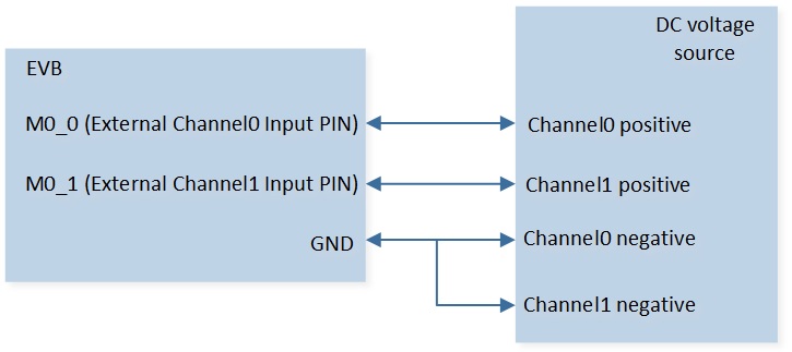
Feature List
VBAT and VADPIN internal channels.
Two external channel input modes: bypass mode and divide mode.
Support single-ended mode.
Two work modes: one shot mode and continuous mode.
16 index schedule table.
TIMER 7 triggers ADC one shot mode sampling.
32 depth FIFO for continuous mode.
Support hardware average function.
Note
RTL87x3D supports 8 external channels. RTL87x3E and RTL87x3EP support 4 external channels. RTL87x3EP doesn’t support continuous mode.
ADC Pin
RTL87x3D supports 8 external channels: external channel 0, 1, 2, 3, 4, 5, 6, and 7 correspond to pin
P0_0,P0_1,P0_2,P0_3,P0_4,P0_5,P0_6, andP0_7.RTL87x3E and RTL87x3EP support 4 external channels: external channel 0, 1, 2, and 3 correspond to pin
P0_0,P0_1,P0_2, andP0_3.
Channel Mode
Single-Ended Mode
Single-Ended mode occupies one channel and uses only one pin for sampling.
Internal VBAT and Internal VADPIN Modes
Internal VBAT mode is used to measure VBAT voltage. Internal VADPIN mode is used to measure VADP voltage.
External Channel Input Mode
Bypass Mode
The input range of ADC bypass mode is 0 to 0.9V.
Divide Mode
The input range of ADC divide mode is 0 to 3.3V.
Work Mode
One Shot Mode
After ADC is enabled, only one sampling is performed. To sample again, the user needs to manually restart sampling.
It can cooperate with TIMER 7 peripheral to realize timing continuous sampling.
Continuous Mode
After ADC is enabled, sampling continues until ADC is disabled.
It can cooperate with GDMA continuous sampling.
ADC Schedule Table Index
ADC has 16 schedule tables. Write the parameters in the table below into schIndex[0] ~ schIndex[15] to set channel mode and channel number.
Then set bitmap, schIndex[0] ~ schIndex[15] corresponding to bit 0 ~ bit 15 of bitmap. If the specific bit of bitmap is set to 1, it means that the schedule table corresponding to this bit is enabled. For example, if config schIndex[0] and schIndex[1], then bitmap is
0000 0000 0011(that is,0x0003), if config schIndex[0] and schIndex[2], then bitmap is0000 0000 0101(that is,0x0005).After ADC is enabled, ADC will sample successively according to the mode configured in the enabled schedule table.
schIndex |
Description |
|---|---|
EXT_SINGLE_ENDED(0) |
Single-Ended mode, the input is external channel 0. |
EXT_SINGLE_ENDED(1) |
Single-Ended mode, the input is external channel 1. |
EXT_SINGLE_ENDED(2) |
Single-Ended mode, the input is external channel 2. |
EXT_SINGLE_ENDED(3) |
Single-Ended mode, the input is external channel 3. |
EXT_SINGLE_ENDED(4) |
Single-Ended mode, the input is external channel 4. |
EXT_SINGLE_ENDED(5) |
Single-Ended mode, the input is external channel 5. |
EXT_SINGLE_ENDED(6) |
Single-Ended mode, the input is external channel 6. |
EXT_SINGLE_ENDED(7) |
Single-Ended mode, the input is external channel 7. |
INTERNAL_VBAT_MODE |
Internal battery voltage detection channel. |
INTERNAL_VADPIN_MODE |
Internal adapter voltage detection channel. |
ADC One Shot Mode Operation Flow
Polling Mode
The flow of ADC sampling in one shot mode by polling is shown in the following figure.

The codes below demonstrate the flow of ADC sampling in one shot mode by polling. For details, please refer to src\sample\io_demo\adc\one-shot\adc_polling_demo.c.
Note
To use the method below, please turn off ‘Charger auto enable’ and ‘Battery detection support’ on the MCUConfig Tool. As shown in Turn Off Charger on the MCUConfig Tool.
/* Enable ADC clock */
RCC_PeriphClockCmd(APBPeriph_ADC, APBPeriph_ADC_CLOCK, ENABLE);

ADC_InitTypeDef adc_init_struct;
/* Fill each ADC_InitStruct member variable with its default value */
ADC_StructInit(&adc_init_struct);

/* Write the parameters into schedule table to set channel mode and channel number. */
adc_init_struct.schIndex[0] = EXT_SINGLE_ENDED(1);
adc_init_struct.schIndex[1] = INTERNAL_VBAT_MODE;
adc_init_struct.schIndex[2] = INTERNAL_VADPIN_MODE;
/* Set bitmap, schIndex[0] ~ schIndex[15] corresponding to bit0 ~ bit15 of bitmap.
   If the specific bit of bitmap is set to 1, it means that the schedule table corresponding to this bit is enabled.
   For example, if config schIndex[0] and schIndex[1], then bitmap is 0000 0000 0011 (that is, 0x0003),
   if config schIndex[0] and schIndex[2], then bitmap is 0000 0000 0101 (that is, 0x0005).
   After ADC is enabled, ADC will sample successively according to the mode configured in the enabled schedule table.
   */
adc_init_struct.bitmap = 0x07;
/* Initialize ADC */
ADC_Init(ADC, &adc_init_struct);

/* Enable ADC one shot mode done interrupt */
ADC_INTConfig(ADC, ADC_INT_ONE_SHOT_DONE, ENABLE);

/* Disable NVIC of ADC */
NVIC_InitTypeDef NVIC_InitStruct;
NVIC_InitStruct.NVIC_IRQChannel = ADC_IRQn;
NVIC_InitStruct.NVIC_IRQChannelPriority = 3;
NVIC_InitStruct.NVIC_IRQChannelCmd = DISABLE;
NVIC_Init(&NVIC_InitStruct);

/* Enable ADC one shot sampling.
   When ADC is enabled, sampling will be done quickly.
   After initialization, ADC can be enabled when sampling is needed. */
ADC_Cmd(ADC, ADC_One_Shot_Mode, ENABLE);

/* Check ADC_INT_ONE_SHOT_DONE interrupt status flag */
while (ADC_GetIntFlagStatus(ADC, ADC_INT_ONE_SHOT_DONE) == RESET);

/* Clear ADC_INT_ONE_SHOT_DONE interrupt */
ADC_ClearINTPendingBit(ADC, ADC_INT_ONE_SHOT_DONE);

/* ADC one shot sampling mode, read data from schedule table.
   The schedule table index which config in ADC init function.
   The value is 0 ~ 15 */
data[0] = ADC_Read(ADC, 0);
data[1] = ADC_Read(ADC, 1);
data[2] = ADC_Read(ADC, 2);

/* Get conversion results based on data. The unit of the result is mV. */
res[0] = ADC_GetRes(data[0], EXT_SINGLE_ENDED(1));
res[1] = ADC_GetRes(data[1], INTERNAL_VBAT_MODE);
res[2] = ADC_GetRes(data[2], INTERNAL_VADPIN_MODE);
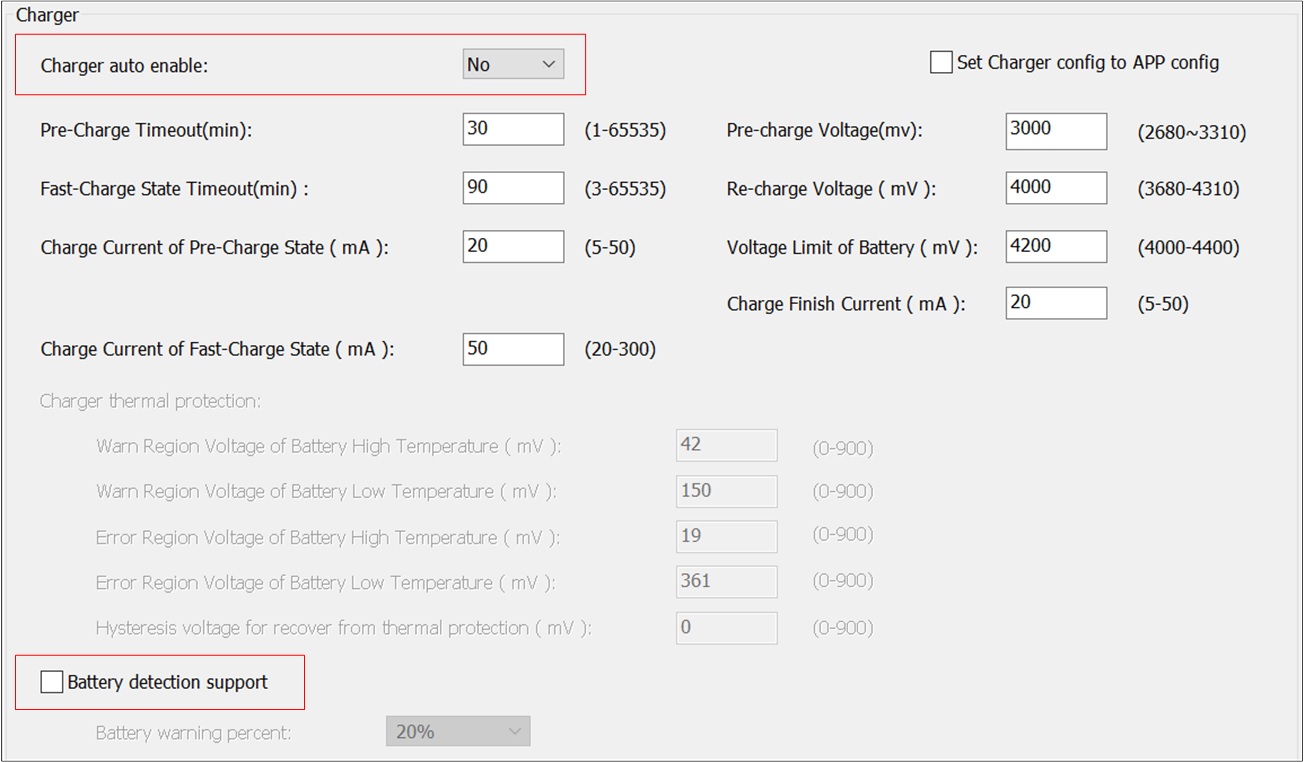
Interrupt Mode
The flow of ADC sampling in one shot mode by interrupt is shown in the following figure.

The codes below demonstrate the flow of ADC sampling in one shot mode by interrupt. For details, please refer to src\sample\io_demo\adc\one-shot\adc_demo.c.
Note
To use the method below, please turn off ‘Charger auto enable’ and ‘Battery detection support’ on the MCUConfig Tool.
/* Bypass mode config, please notice that the input voltage of
   ADC channel using bypass mode should not be over 0.9V */
ADC_HighBypassCmd(1, ENABLE);

/* Enable ADC clock */
RCC_PeriphClockCmd(APBPeriph_ADC, APBPeriph_ADC_CLOCK, ENABLE);

ADC_InitTypeDef adcInitStruct;
/* Fill each ADC_InitStruct member variable with its default value */
ADC_StructInit(&adcInitStruct);

/* Write the parameters into schedule table to set channel mode and channel number. */
adcInitStruct.schIndex[0] = EXT_SINGLE_ENDED(0);
adcInitStruct.schIndex[1] = EXT_SINGLE_ENDED(1);
adcInitStruct.schIndex[2] = INTERNAL_VBAT_MODE;
adcInitStruct.schIndex[3] = INTERNAL_VADPIN_MODE;
/* Set bitmap, schIndex[0] ~ schIndex[15] corresponding to bit0 ~ bit15 of bitmap.
   If the specific bit of bitmap is set to 1, it means that the schedule table corresponding to this bit is enabled.
   For example, if config schIndex[0] and schIndex[1], then bitmap is 0000 0000 0011 (that is, 0x0003).
   If config schIndex[0] and schIndex[2], then bitmap is 0000 0000 0101 (that is, 0x0005).
   After ADC is enabled, ADC will sample successively according to the mode configured in the enabled schedule table.
   */
adcInitStruct.bitmap = 0x0f;
/* Initialize ADC */
ADC_Init(ADC, &adcInitStruct);

/* Enable ADC one shot mode done interrupt */
ADC_INTConfig(ADC, ADC_INT_ONE_SHOT_DONE, ENABLE);

/* Enable NVIC of ADC */
NVIC_InitTypeDef NVIC_InitStruct;
NVIC_InitStruct.NVIC_IRQChannel = ADC_IRQn;
NVIC_InitStruct.NVIC_IRQChannelPriority = 2;
NVIC_InitStruct.NVIC_IRQChannelCmd = ENABLE;
NVIC_Init(&NVIC_InitStruct);

/* Enable ADC one shot sampling.
   When ADC is enabled, sampling will be done quickly and interruption will occur.
   After initialization, ADC can be enabled when sampling is needed. */
ADC_Cmd(ADC, ADC_One_Shot_Mode, ENABLE);
ADC interrupt handle flow is shown in the following figure.
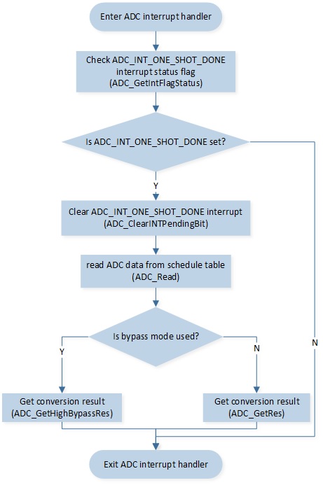
The codes below demonstrate the ADC interrupt handle flow.
void adc_handler(void)
{
    int32_t data[4];
    int32_t res[4];

    /* Check ADC_INT_ONE_SHOT_DONE interrupt status flag */
    if (ADC_GetIntFlagStatus(ADC, ADC_INT_ONE_SHOT_DONE) == SET)
    {
        /* Clear ADC_INT_ONE_SHOT_DONE interrupt */
        ADC_ClearINTPendingBit(ADC, ADC_INT_ONE_SHOT_DONE);
        /* ADC one shot sampling mode, read data from schedule table.
           The schedule table index which config in ADC_Init function.
           The value is 0 ~ 15 */
        data[0] = ADC_Read(ADC, 0);
        data[1] = ADC_Read(ADC, 1);
        data[2] = ADC_Read(ADC, 2);
        data[3] = ADC_Read(ADC, 3);
        /* Get conversion results based on data. The unit of the result is mV. */
        res[0] = ADC_GetRes(data[0], EXT_SINGLE_ENDED(0));
        res[1] = ADC_GetHighBypassRes(data[1], EXT_SINGLE_ENDED(1));
        res[2] = ADC_GetRes(data[2], INTERNAL_VBAT_MODE);
        res[3] = ADC_GetRes(data[3], INTERNAL_VADPIN_MODE);
    }
}
Hardware Average Mode
ADC hardware average function can only be used in one shot mode and only schedule table 0 can be used. For RTL87x3E and RTL87x3EP, it is recommended to use the hardware average function. The flow of ADC sampling in one shot mode by hardware average is shown in the following figure.

The codes below demonstrate the flow of ADC sampling in one shot mode by hardware average. For details, please refer to src\sample\io_demo\adc\adc_hw_average\adc_hw_average_demo.c.
Note
To use the method below, please turn off ‘Charger auto enable’ and ‘Battery detection support’ on the MCUConfig Tool.
/* Enable ADC clock */
RCC_PeriphClockCmd(APBPeriph_ADC, APBPeriph_ADC_CLOCK, ENABLE);

ADC_InitTypeDef adc_init_struct;
/* Fill each ADC_InitStruct member variable with its default value */
ADC_StructInit(&adc_init_struct);

/* When hardware average function is enabled, ADC can only use schedule table 0 */
adc_init_struct.schIndex[0] = EXT_SINGLE_ENDED(1);
adc_init_struct.bitmap = 0x01;
/* Initialize ADC */
ADC_Init(ADC, &adc_init_struct);

/* Enable ADC hardware average function */
ADC_HwEvgEn(ADC, ENABLE);
/* Set the hardware average number of times */
ADC_HwEvgSel(ADC, ADC_DTAT_AVG_SEL_BY32);

/* Enable ADC one shot mode done interrupt */
ADC_INTConfig(ADC, ADC_INT_ONE_SHOT_DONE, ENABLE);

/* Enable NVIC of ADC */
NVIC_InitTypeDef NVIC_InitStruct;
NVIC_InitStruct.NVIC_IRQChannel = ADC_IRQn;
NVIC_InitStruct.NVIC_IRQChannelPriority = 3;
NVIC_InitStruct.NVIC_IRQChannelCmd = ENABLE;
NVIC_Init(&NVIC_InitStruct);

/* Enable ADC one shot sampling.
   When ADC is enabled, sampling will be done quickly and interruption will occur.
   After initialization, ADC can be enabled when sampling is needed. */
ADC_Cmd(ADC, ADC_One_Shot_Mode, ENABLE);
ADC interrupt handle flow is shown in the following figure.
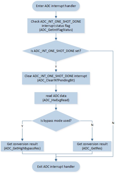
The codes below demonstrate the ADC interrupt handle flow.
void adc_handler(void)
{
    int32_t data;
    int32_t result;

    /* Check ADC_INT_ONE_SHOT_DONE interrupt status flag */
    if (ADC_GetIntFlagStatus(ADC, ADC_INT_ONE_SHOT_DONE) == SET)
    {
        /* Clear ADC_INT_ONE_SHOT_DONE interrupt */
        ADC_ClearINTPendingBit(ADC, ADC_INT_ONE_SHOT_DONE);
        /* Read ADC data */
        data = ADC_HwEvgRead(ADC);
        /* Get conversion results based on data. The unit of the result is mV. */
        result = ADC_GetRes(data, EXT_SINGLE_ENDED(1));
    }
}
ADC Manager Mode
When the internal charger is enabled, it is necessary to use adc manager mode for ADC sampling. The flow of ADC sampling in one shot mode by ADC manager is shown in the following figure.

The codes below demonstrate the flow of ADC sampling in one shot mode by ADC manager. For details, please refer to src\sample\io_demo\adc\adc_charger_demo\adc_charger_demo.c and src\sample\io_demo\adc\adc_manger\adc_manager_demo.c.
Note
To use the method below, please turn on ‘Charger auto enable’ and ‘Battery detection support’ on the MCUConfig Tool.
/* Bypass mode config, please notice that the input voltage of
   ADC channel using bypass mode should not be over 0.9V */
ADC_HighBypassCmd(0, ENABLE);
ADC_HighBypassCmd(1, ENABLE);

ADC_InitTypeDef ADC_InitStruct;
/* Fill each ADC_InitStruct member variable with its default value */
ADC_StructInit(&ADC_InitStruct);

/* Set bitmap, schIndex[0] ~ schIndex[15] corresponding to bit0 ~ bit15 of bitmap.
   If the specific bit of bitmap is set to 1, it means that the schedule table corresponding to this bit is enabled.
   For example, if config schIndex[0] and schIndex[1], then bitmap is 0000 0000 0011 (that is, 0x0003),
   if config schIndex[0] and schIndex[2], then bitmap is 0000 0000 0101 (that is, 0x0005).
   After ADC is enabled, ADC will sample successively according to the mode configured in the enabled schedule table.
   */
ADC_InitStruct.bitmap = 0x0007;
/* Write the parameters into schedule table to set channel mode and channel number. */
ADC_InitStruct.schIndex[0] = EXT_SINGLE_ENDED(0);
ADC_InitStruct.schIndex[1] = EXT_SINGLE_ENDED(1);
ADC_InitStruct.schIndex[2] = INTERNAL_VBAT_MODE;

/* Request for a channel in ADC manager */
if (!adc_mgr_register_req(&ADC_InitStruct,
                              (adc_callback_function_t)app_adc_vbat_ntc_voltage_read_callback,
                              &adc_channel_vbat_ntc_voltage))
{
    IO_PRINT_ERROR0("app_adc_vbat_ntc_voltage_init: adc_mgr_register_req failed");
}

/* Enable the specific ADC manager channel for sampling */
adc_mgr_enable_req(adc_channel_vbat_ntc_voltage);
ADC manager callback handle flow is shown in the following figure.
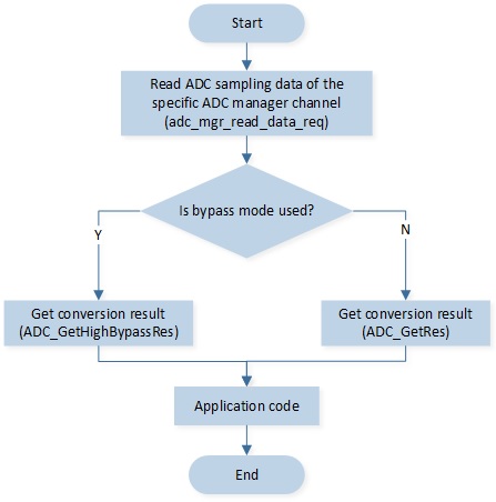
The codes below demonstrate the ADC manager callback handle flow.
static void app_adc_vbat_ntc_voltage_read_callback(void *pvPara, uint32_t int_status)
{
    uint16_t adc_data[3];
    uint16_t sched_bit_map = 0x0007;

    /* Read ADC sampling data of the specific ADC manager channel */
    adc_mgr_read_data_req(adc_channel_vbat_ntc_voltage, adc_data, sched_bit_map);

    /* Get conversion results based on data. The unit of the result is mV. */
    adc_charger_data_mgr.temperature_battery_1 = ADC_GetHighBypassRes(adc_data[0], EXT_SINGLE_ENDED(0));
    adc_charger_data_mgr.temperature_battery_2 = ADC_GetHighBypassRes(adc_data[1], EXT_SINGLE_ENDED(1));
    adc_charger_data_mgr.voltage_battery = ADC_GetRes(adc_data[2], INTERNAL_VBAT_MODE);
}
ADC Continuous Mode Operation Flow
GDMA Mode
The flow of ADC sampling in continuous mode by GDMA is shown in the following figure.

The codes below demonstrate the flow of ADC sampling in continuous mode by GDMA. For details, please refer to src\sample\io_demo\gdma\adc_dma\adc_gdma_demo.c.
Note
To use the method below, please turn off ‘Charger auto enable’ and ‘Battery detection support’ on the MCUConfig Tool.
Please refer to
src\sample\io_demo\adc\adc_continuous_mode\adc_continuous_mode_demo.cfor use of the internal charger and ADC continuous sampling mode at the same time.
/* Enable ADC clock */
RCC_PeriphClockCmd(APBPeriph_ADC, APBPeriph_ADC_CLOCK, ENABLE);

ADC_InitTypeDef adc_init_struct;
/* Fill each ADC_InitStruct member variable with its default value */
ADC_StructInit(&adc_init_struct);

/* Write the parameters into schedule table to set channel mode and channel number. */
adc_init_struct.schIndex[0] = EXT_SINGLE_ENDED(0);
/* Set bitmap, schIndex[0] ~ schIndex[15] corresponding to bit0 ~ bit15 of bitmap.
   If the specific bit of bitmap is set to 1, it means that the schedule table corresponding to this bit is enabled.
   For example, if config schIndex[0] and schIndex[1], then bitmap is 0000 0000 0011 (that is, 0x0003),
   if config schIndex[0] and schIndex[2], then bitmap is 0000 0000 0101 (that is, 0x0005).
   After ADC is enabled, ADC will sample successively according to the mode configured in the enabled schedule table.
    */
adc_init_struct.bitmap = 0x01;
/* Set burst size to trigger GDMA request */
adc_init_struct.adcBurstSize = 8;
/* Initialize ADC */
ADC_Init(ADC, &adc_init_struct);
SLEEP LED
SLEEP LED Demo Code Support List
Demo 1 |
sleep_led_demo.c |
|---|---|
Sample Purpose |
Demonstrate SLEEP LED breathe mode. |
File Path |
|
Function Entry |
|
Phase0 Parameters |
Duty update time: 10ms |
Phase1 Parameters |
Duty update time: 10ms |
Phase2 Parameters |
Duty update time: 10ms |
Phase3 Parameters |
Duty update time: 10ms |
Phase4 Parameters |
Duty update time: 10ms |
Phase5 Parameters |
Duty update time: 10ms |
Phase6 Parameters |
Duty update time: 10ms |
Phase7 Parameters |
Duty update time: 10ms |
Hardware Connection |
As shown in SLEEP LED Demo Hardware Connection Diagram. On EVB, connect M0_1 to LED1 and connect M2_1 to LED2 and connect M2_2 to LED3. |
Pin Definition |
|
Expected Result |
LEDs turn from dark to bright and then from bright to dark in breathe mode. |
Demo 2 |
sleep_led_demo.c |
|---|---|
Sample Purpose |
Demonstrate SLEEP LED blink mode. |
File Path |
|
Function Entry |
|
Period Parameters |
Channel0: period0, period1, and period2 high level time is 200ms, period0, period1, and period2 low level time is 100ms. |
Hardware Connection |
As shown in SLEEP LED Demo Hardware Connection Diagram. On EVB, connect M0_1 to LED1 and connect M2_1 to LED2 and connect M2_2 to LED3. |
Pin Definition |
|
Expected Result |
LEDs blink with 200ms on and 100ms off. |
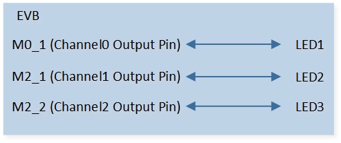
Function Description
SLEEP LED is used to control LED to make the effect of blinking light or breathing light.
Note
RTL87x3D and RTL87x3E support SLEEP LED. RTL87x3EP doesn’t support SLEEP LED.
Feature List
Support three channels.
Support blink mode and breathe mode.
32KHz clock source.
3 periods per channel in blink mode.
8 phases per channel in breathe mode.
Support output level setting in idle state.
Support reverse output function.
Support period bypass in blink mode and phase bypass in breathe mode.
Note
If a default pull-up pin (P1_0/P1_1/P2_0/P3_0/P3_1) is set as a high active LED, or any other pull-down pin is set as a low active LED, it will blink when CPU reboots.
Blink Mode
In blink mode, one channel is divided into three periods. As shown in the following figure, it is executed sequentially from period0, and after the end of period2, it goes back to period0 to continue the loop execution.
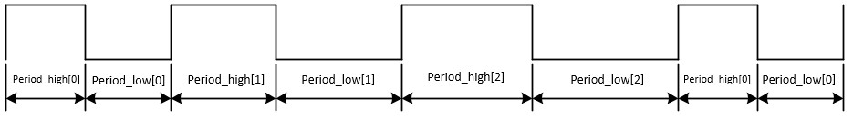
Note
period_timetick = prescale / 32000
periodx high level time = period_high[x] * period_timetick (x = 0, 1, 2)
periodx low level time = period_low[x] * period_timetick (x = 0, 1, 2)
If period_high[x] or period_low[x] is 0, this and subsequent periods are bypassed. For example, if period_high[2] is 0, period2 is bypassed, it is executed sequentially from period0, and after the end of period1, it goes to period0 to continue the loop execution.
Breathe Mode
In breathe mode, one channel is divided into eight phases. As shown in the following figure, it is executed sequentially from phase0, and after the end of phase7, it goes to phase0 to continue the loop execution.
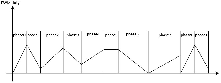
Note
phase_timetick = prescale / 32000
phase_uptate_rate[x]: duty update time = (phase_uptate_rate[x] + 1) * phase_timetick (x = 0, 1, 2, …, 7)
phase_phase_tick[x]: The duration of the whole phase. phasex output time = phase_phase_tick[x] * phase_timetick (x = 0, 1, 2, …, 7)
phase_initial_duty[x]: initial high level time = phase_initial_duty[x] / 32000 (x = 0, 1, 2, …, 7)
phase_increase_duty[x]: The direction of each change of duty. 1: increase duty. 0: decrease duty. (x = 0, 1, 2, …, 7)
phase_duty_step[x]: duty step time = phase_duty_step[x] / 32000 (x = 0, 1, 2, …, 7)
After high level time increases to phase_timetick, it remains at phase_timetick.
After high level time decreases to 0, it remains at 0.
Low level time = phase_timetick - high level time
If phase_phase_tick[x] is 0, this and subsequent phases are bypassed. For example, if phase_phase_tick[6] is 0, phase6 and phase7 are bypassed, it is executed sequentially from phase0, and after the end of phase5, it goes to phase0 to continue the loop execution.
Idle State
Call the SleepLed_SetIdleMode() API to set whether the channel outputs a high level or low level after the SLEEP LED is disabled.
Reverse Output Function
Each channel of SLEEP LED supports the reverse function. After the reverse function is enabled, the original waveform is reversed and output, the actual waveform is opposite to the set value.
Blink Mode Operation Flow
The operation flow of SLEEP LED blink mode is shown in the following figure.
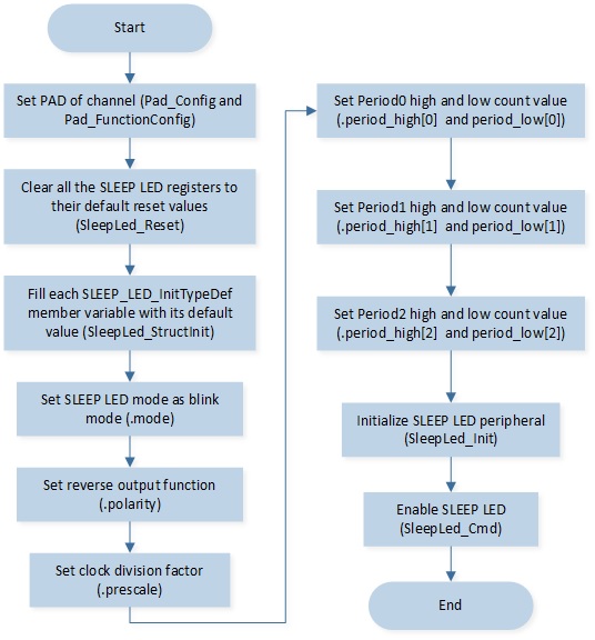
The codes below demonstrate the SLEEP LED blink mode operation flow.
/* Clear all the SLEEP LED registers to their default reset values */
SleepLed_Reset();

SLEEP_LED_InitTypeDef Led_Initsturcture;
/* Fill each SLEEP_LED_InitTypeDef member variable with its default value */
SleepLed_StructInit(&Led_Initsturcture);

/* Set SLEEP LED mode */
Led_Initsturcture.mode                        = LED_BLINK_MODE;
/* Set reverse output function */
Led_Initsturcture.polarity                    = LED_OUTPUT_NORMAL;
/* Set clock division factor */
Led_Initsturcture.prescale                    = 32;
/* Set period0 high and low count value */
Led_Initsturcture.period_high[0]              = 200;
Led_Initsturcture.period_low[0]               = 100;
/* Set period1 high and low count value */
Led_Initsturcture.period_high[1]              = 200;
Led_Initsturcture.period_low[1]               = 100;
/* Set period2 high and low count value */
Led_Initsturcture.period_high[2]              = 200;
Led_Initsturcture.period_low[2]               = 100;
/* Initialize channel 0 */
SleepLed_Init(LED_CHANNEL_0, &Led_Initsturcture);

Led_Initsturcture.period_high[2]              = 0;
Led_Initsturcture.period_low[2]               = 0;
/* Initialize channel 1 */
SleepLed_Init(LED_CHANNEL_1, &Led_Initsturcture);

Led_Initsturcture.period_high[1]              = 0;
Led_Initsturcture.period_low[1]               = 0;
/* Initialize channel 2 */
SleepLed_Init(LED_CHANNEL_2, &Led_Initsturcture);
/* Enable Sleep led */
SleepLed_Cmd(LED_CHANNEL_1 | LED_CHANNEL_0 | LED_CHANNEL_2, ENABLE);
Breathe Mode Operation Flow
The operation flow of SLEEP LED breathe mode is shown in the following figure.
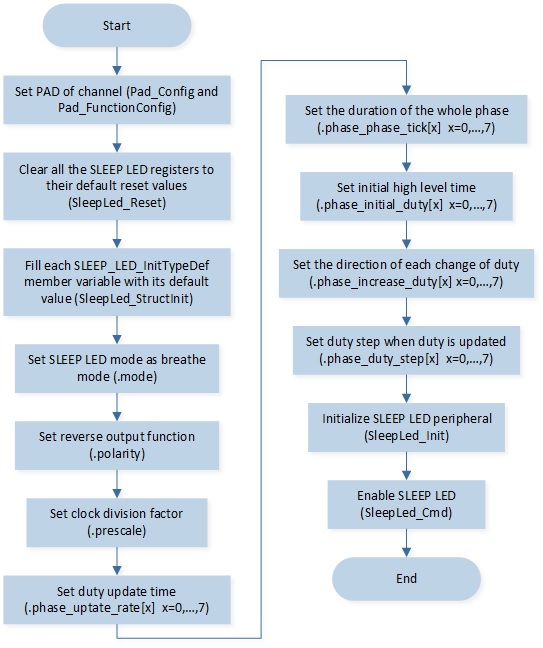
The codes below demonstrate the SLEEP LED breathe mode operation flow.
/* Clear all the Sleep LED registers to their default reset values */
SleepLed_Reset();

SLEEP_LED_InitTypeDef Led_Initsturcture;
/* Fill each SLEEP_LED_InitTypeDef member variable with its default value */
SleepLed_StructInit(&Led_Initsturcture);

/* Set clock division factor */
Led_Initsturcture.prescale                    = 320;
/* Set SLEEP LED mode */
Led_Initsturcture.mode                        = LED_BREATHE_MODE;
/* Set reverse output function */
Led_Initsturcture.polarity                    = LED_OUTPUT_NORMAL;
/* Set duty update time */
Led_Initsturcture.phase_uptate_rate[0]              = 0;
/* Set the duration of the whole phase */
Led_Initsturcture.phase_phase_tick[0]               = 50;
/* Set initial high level time */
Led_Initsturcture.phase_initial_duty[0]             = 0;
/* Set the direction of each change of duty */
Led_Initsturcture.phase_increase_duty[0]            = 1;
/* Set duty step when duty is updated */
Led_Initsturcture.phase_duty_step[0]                = 1;

/* Set phase1 parameters */
Led_Initsturcture.phase_uptate_rate[1]              = 0;
Led_Initsturcture.phase_phase_tick[1]               = 50;
Led_Initsturcture.phase_initial_duty[1]             = 100;
Led_Initsturcture.phase_increase_duty[1]            = 1;
Led_Initsturcture.phase_duty_step[1]                = 2;

/* Set phase2 parameters */
Led_Initsturcture.phase_uptate_rate[2]              = 0;
Led_Initsturcture.phase_phase_tick[2]               = 50;
Led_Initsturcture.phase_initial_duty[2]             = 200;
Led_Initsturcture.phase_increase_duty[2]            = 1;
Led_Initsturcture.phase_duty_step[2]                = 3;

/* Set phase3 parameters */
Led_Initsturcture.phase_uptate_rate[3]              = 0;
Led_Initsturcture.phase_phase_tick[3]               = 50;
Led_Initsturcture.phase_initial_duty[3]             = 300;
Led_Initsturcture.phase_increase_duty[3]            = 1;
Led_Initsturcture.phase_duty_step[3]                = 4;

/* Set phase4 parameters */
Led_Initsturcture.phase_uptate_rate[4]              = 0;
Led_Initsturcture.phase_phase_tick[4]               = 50;
Led_Initsturcture.phase_initial_duty[4]             = 300;
Led_Initsturcture.phase_increase_duty[4]            = 0;
Led_Initsturcture.phase_duty_step[4]                = 1;

/* Set phase5 parameters */
Led_Initsturcture.phase_uptate_rate[5]              = 0;
Led_Initsturcture.phase_phase_tick[5]               = 50;
Led_Initsturcture.phase_initial_duty[5]             = 200;
Led_Initsturcture.phase_increase_duty[5]            = 0;
Led_Initsturcture.phase_duty_step[5]                = 2;

/* Set phase6 parameters */
Led_Initsturcture.phase_uptate_rate[6]              = 0;
Led_Initsturcture.phase_phase_tick[6]               = 50;
Led_Initsturcture.phase_initial_duty[6]             = 100;
Led_Initsturcture.phase_increase_duty[6]            = 0;
Led_Initsturcture.phase_duty_step[6]                = 3;

/* Set phase7 parameters */
Led_Initsturcture.phase_uptate_rate[7]              = 0;
Led_Initsturcture.phase_phase_tick[7]               = 50;
Led_Initsturcture.phase_initial_duty[7]             = 0;
Led_Initsturcture.phase_increase_duty[7]            = 0;
Led_Initsturcture.phase_duty_step[7]                = 0;
/* Initialize channel 0 */
SleepLed_Init(LED_CHANNEL_0, &Led_Initsturcture);
/* Initialize channel 1 */
SleepLed_Init(LED_CHANNEL_1, &Led_Initsturcture);
/* Initialize channel 2 */
SleepLed_Init(LED_CHANNEL_2, &Led_Initsturcture);
/* Enable Sleep led */
SleepLed_Cmd(LED_CHANNEL_1 | LED_CHANNEL_0 | LED_CHANNEL_2, ENABLE);
QDEC
QDEC Demo Code Support List
Demo 1 |
qdec_demo.c |
|---|---|
Sample Purpose |
Demonstrate how QDEC works. |
Brief Introduction |
This sample code demonstrates how QDEC works. The chip will detect the direction and count of wheel turns. |
File Path |
|
Function Entry |
|
Hardware Connection |
As shown in QDEC Demo Hardware Connection Diagram. On EVB, connect P1_0 to the PHA of the wheel, connect P1_1 to the PHB of the wheel. |
QDEC PHA Pin Definition |
|
QDEC PHB Pin Definition |
|
QDEC Axial |
Y |
Scan Clock |
50KHz |
Debounce Clock |
5KHz |
Debounce |
Enable |
Debounce Time |
5ms |
Expected Result |
1. Press the reset button on the EVB. |
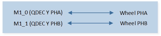
Function Description
As shown in the following figure, QDEC is used to detect the motion state of the rotation-sensing device. When the rotating device moves, it will output two quadrature signals PHA and PHB. QDEC judges the direction of rotation by detecting the phase change of PHA and PHB.

Feature List
Support 3 axes.
Support hardware debounce: debounce time for each axis can be set independently.
Support initial phase setting.
Support illegal phase change detection.
16-bit phase change counter.
Note
RTL87x3E cannot disable the hardware debounce function. RTL87x3D can disable the hardware debounce function.
Direction Judgment and Counting Method
PHA and PHB are combined into a 2-bit number. PHA is the high bit, and PHB is the low bit.
The phases are divided into four types: 00, 01, 11, and 10.
As shown in the following figure, changes in the order of 00, 01, 11, and 10 are defined as positive. When the counter scale is set to 0, the counter will increase by one when the phase changes once. When the counter scale is set to 1, the counter will increase by one when the phase changes twice.
Changes in the order of 00, 10, 11, and 01 are defined as negative. When the counter scale is set to 0, the counter will decrease by one when the phase changes once. When the counter scale is set to 1, the counter will decrease by one when the phase changes twice.
PHA and PHB should only have one signal change at a time. If both signals change at the same time, the state is considered wrong. When this error state occurs, the counter does not count. Illegal interrupts can be turned on to detect this error condition.
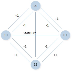
QDEC Operation Flow
QDEC operation flow is shown in the following figure.
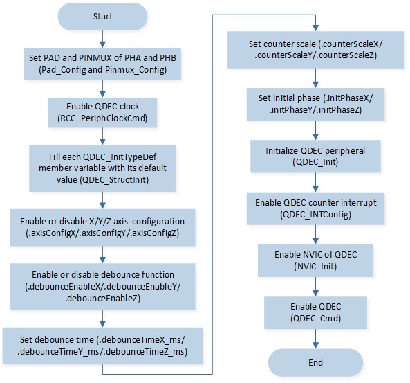
The codes below demonstrate the QDEC operation flow.
RCC_PeriphClockCmd(APBPeriph_QDEC, APBPeriph_QDEC_CLOCK, ENABLE);

QDEC_InitTypeDef qdecInitStruct;
QDEC_StructInit(&qdecInitStruct);
qdecInitStruct.ScanClockKHZ         = 50; /*!< 50KHz */
qdecInitStruct.DebonceClockKHZ     = 5; /*!< 5KHz */
qdecInitStruct.axisConfigY       = ENABLE;
qdecInitStruct.debounceEnableY   = Debounce_Enable;
qdecInitStruct.debounceTimeY     = 5 * 5; /*!< 5ms */

QDEC_Init(QDEC, &qdecInitStruct);

RamVectorTableUpdate(Qdecode_VECTORn, (IRQ_Fun)qdec_handler);
QDEC_INTConfig(QDEC, QDEC_Y_INT_NEW_DATA, ENABLE);

NVIC_InitTypeDef nvic_init_struct;
nvic_init_struct.NVIC_IRQChannel         = QDEC_IRQn;
nvic_init_struct.NVIC_IRQChannelCmd      = (FunctionalState)ENABLE;
nvic_init_struct.NVIC_IRQChannelPriority = 3;
NVIC_Init(&nvic_init_struct);

QDEC_Cmd(QDEC, QDEC_AXIS_Y, ENABLE);
QDEC interrupt handle flow is shown in the following figure.
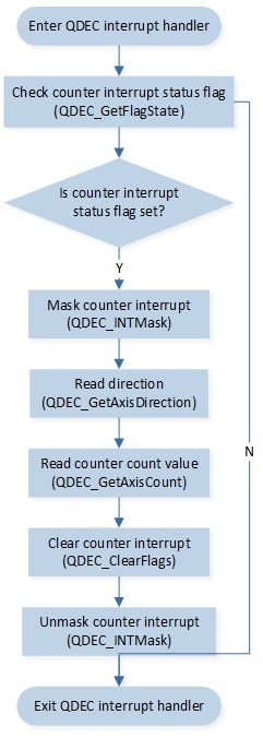
The codes below demonstrate the QDEC interrupt handle flow.
void qdec_handler(void)
{
    /* Check Y-axis counter interrupt status flag */
    if (QDEC_GetFlagState(QDEC, QDEC_FLAG_NEW_CT_STATUS_Y) == SET)
    {
        /* Mask Y-axis counter interrupt */
        QDEC_INTMask(QDEC, QDEC_Y_CT_INT_MASK, ENABLE);

        /* Read direction */
        dir = QDEC_GetAxisDirection(QDEC, QDEC_AXIS_Y);
        /* Read counter count value */
        y_axis = QDEC_GetAxisCount(QDEC, QDEC_AXIS_Y);
        IO_PRINT_INFO2("qdec_handler: dir %d, y_axis %d", dir, y_axis);
        /* clear Y-axis counter interrupt status flag */
        QDEC_ClearFlags(QDEC, QDEC_CLR_NEW_CT_Y);
        /* Unmask Y-axis counter interrupt */
        QDEC_INTMask(QDEC, QDEC_Y_CT_INT_MASK, DISABLE);
    }
}
KeyScan
KeyScan Demo Code Support List
Demo 1 |
keyscan_demo.c |
|---|---|
Sample Purpose |
Demonstrates that KeyScan works in active mode. |
File Path |
|
Function Entry |
|
Hardware Connection |
As shown in KeyScan Hardware Connection Diagram. EVB is connected to matrix keyboard module: connect M0_2 to ROW0, M0_3 to ROW1, M0_0 to COLUMN0, and M0_1 to COLUMN1. |
Pin Definition |
|
Expected Result |
1. When a key is pressed, key information is printed on Debug Analyzer. |
Demo 2 |
keyscan_demo_dlps.c |
|---|---|
Sample Purpose |
Demonstrates that KeyScan works in DLPS mode. |
File Path |
|
Function Entry |
|
Hardware Connection |
As shown in KeyScan Hardware Connection Diagram. EVB is connected to matrix keyboard module: connect M0_2 to ROW0, M0_3 to ROW1, M0_0 to COLUMN0, and M0_1 to COLUMN1. |
Pin Definition |
|
Expected Result |
1. Press the reset button on the EVB, the string ‘io_dlps_enter’ will be printed on Debug Analyzer and the system will enter DLPS mode. |
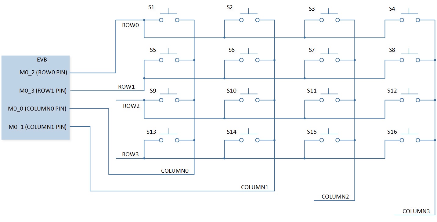
Function Description
KeyScan needs to be used with an external key matrix. In the idle state, row[x] is input, pull high is required, column[y] is output low, and output mode must be open-drain. When any key is pressed, the level of the corresponding row changes from high to low, triggering KeyScan hardware scan action.
After the debounce is completed, the first scan starts. When scanning, the column[y] being scanned is output low, and the other columns output high. If row[x] is low at this time, it is considered that row[x] column[y] key is pressed.
Scan order is first column[0] fixed, scan from row[0] to row[x], then column[1] fixed, scan from row[0] to row[x], until column[y].
Note
RTL87x3D and RTL87x3E support KeyScan, RTL87x3EP doesn’t support KeyScan.
Feature List
Support 12 (row) * 20 (column) matrix scan.
Configurable number of rows (1-12), columns (1-20).
Support hardware debounce, configurable debounce time.
Configurable scan clock.
Support multi-key detection, up to 26 keys can be pressed at the same time.
Support periodic scan, configurable scan period.
26 bytes FIFO depth.
Support auto scan and manual scan.
Support all key release hardware detection.
Clock Divider
IO Clock will be divided into 2 channels.
The KeyScan scan clock is generated by the frequency division of keyscan_clk_div (11 bits), which can be freely configured in the range of 10KHz ~ 100KHz.
The low-level delay clock is generated by the frequency division of keyscan_delay_div (6 bits) for use by the relevant timer.
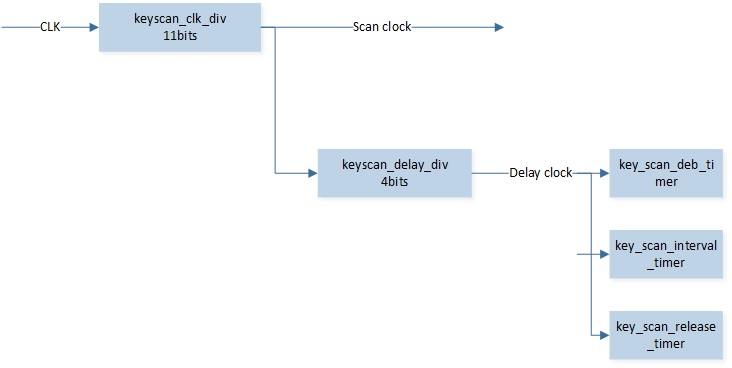
Auto Scan Mode
The workflow of automatic scanning is shown in the figure below.
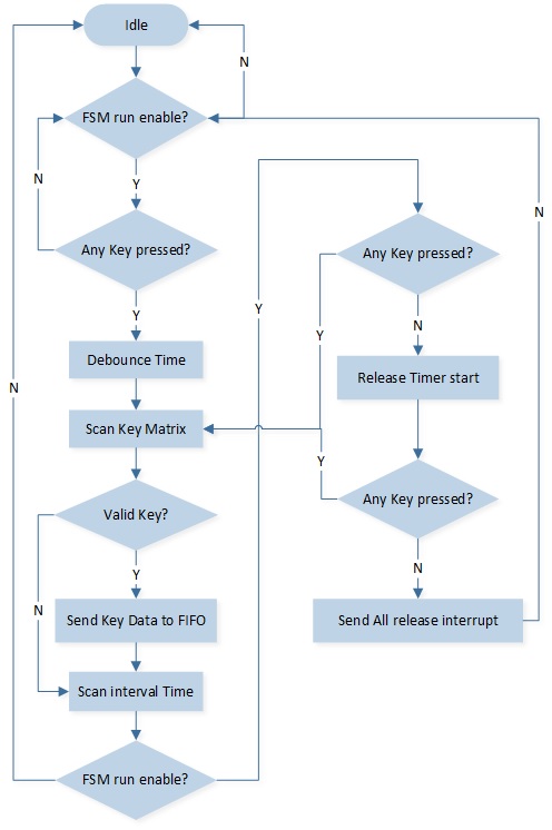
Interrupt
KEYSCAN_INT_OVER_READWhen there is no data in the FIFO, reading the FIFO will trigger this interrupt to prevent over-reading.
KEYSCAN_INT_SCAN_ENDWhether the key value is scanned or not, the interrupt will be triggered as long as the scanning action is completed.
KEYSCAN_INT_FIFO_NOT_EMPTYIf there is data in the FIFO, the interrupt will be triggered.
KEYSCAN_INT_THRESHOLDThis interrupt is triggered when data in the FIFO reaches the threshold level.
KEYSCAN_INT_ALL_RELEASEWhen the release time count reaches the set value, if no key is pressed, the interrupt is triggered.
KeyScan Operation Flow
KeyScan initialization flow is shown in the following figure.
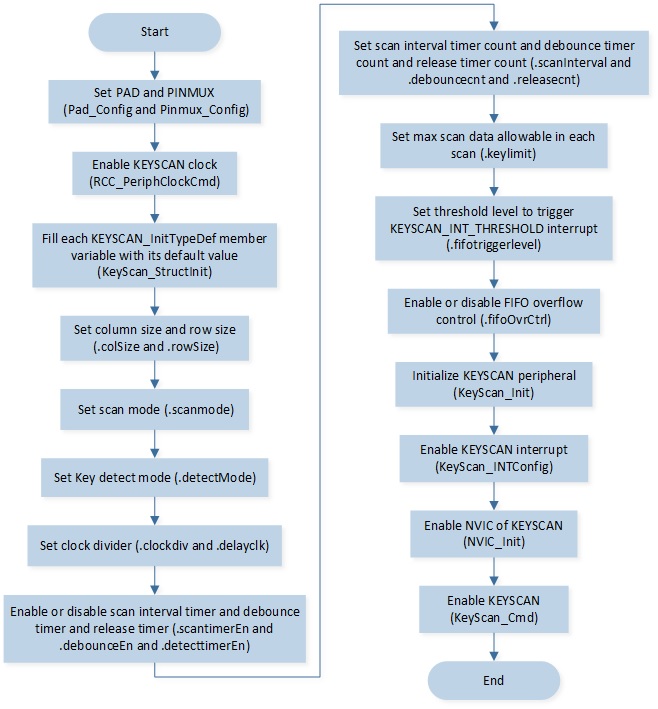
The codes below demonstrate the KeyScan initialization flow.
For details, please refer to src\sample\io_demo\keyscan\active\keyscan_demo.c.
RCC_PeriphClockCmd(APBPeriph_KEYSCAN, APBPeriph_KEYSCAN_CLOCK, ENABLE);
KEYSCAN_InitTypeDef  KeyScan_InitStruct;
KeyScan_StructInit(&KeyScan_InitStruct);
KeyScan_InitStruct.colSize         = KEYPAD_COLUMN_SIZE;
KeyScan_InitStruct.rowSize         = KEYPAD_ROW_SIZE;
KeyScan_InitStruct.scanInterval    = 0x80;
KeyScan_Init(KEYSCAN, &KeyScan_InitStruct);
KeyScan_INTConfig(KEYSCAN, KEYSCAN_INT_SCAN_END | KEYSCAN_INT_ALL_RELEASE, ENABLE);

NVIC_InitTypeDef nvic_init_struct;
nvic_init_struct.NVIC_IRQChannel         = KeyScan_IRQn;
nvic_init_struct.NVIC_IRQChannelCmd      = (FunctionalState)ENABLE;
nvic_init_struct.NVIC_IRQChannelPriority = 3;
NVIC_Init(&nvic_init_struct);

KeyScan_Cmd(KEYSCAN, ENABLE);
I2S
Function Description
I2S interface can support audio protocols such as I2S, Left-Justified, PCM, and TDM. Through the I2S interface, RTL87x3E and RTL87x3D can bridge to an external DSP core (or audio codec/audio amplifier). I2S can be operated in GDMA mode or FIFO mode. Set the buffer size according to the amount of transferred data in GDMA mode, or access I2S FIFO directly to transmit and receive data in FIFO mode. It is recommended to transfer the audio data via GDMA automatically since it can reduce the number of interrupts and improve efficiency.
Feature List
Configurable BCLK and LRCK clock rate.
Support I2S, Left-Justified, PCM format.
Support 16/ 20/ 24/ 32 bits data resolution (data width).
Support 16/ 20/ 24/ 32 bits word length (channel width).
Support non-TDM (2-ch), TDM4 (4-ch), TDM6 (6-ch), and TDM8 (8-ch).
Support master and slave mode.
Support GDMA handshake operation.
Note
RTL87x3D has 4 ports, RTL87x3E has 2 ports.
RTL87x3D supports up to TDM8, RTL87x3E supports up to TDM4.
I2S Initialization Flow
I2S function initialization flow is shown in the following figure.
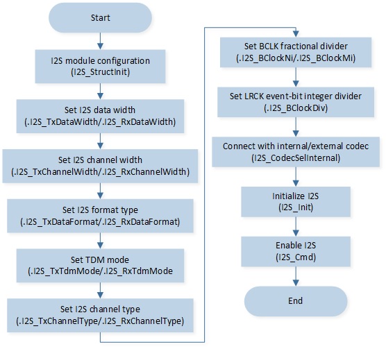
The codes below demonstrate the I2S function initialization flow.
Note
As mentioned in PINMUX and PAD function descriptions, I2S PAD should be configured as software mode and pulled down when I2S is disabled to prevent PAD from floating during low power mode.
void board_i2s_init(void)
{
    /* set PAD_SW_MODE & PAD_PULL_DOWN when I2S is disabled to prevent PAD floating in low power mode */
    Pad_Config(I2S_BCLK_PIN, PAD_PINMUX_MODE, PAD_IS_PWRON, PAD_PULL_NONE, PAD_OUT_ENABLE, PAD_OUT_LOW);
    Pad_Config(I2S_LRCK_PIN, PAD_PINMUX_MODE, PAD_IS_PWRON, PAD_PULL_NONE, PAD_OUT_ENABLE, PAD_OUT_LOW);
    Pad_Config(I2S_SDO_PIN, PAD_PINMUX_MODE, PAD_IS_PWRON, PAD_PULL_NONE, PAD_OUT_ENABLE, PAD_OUT_LOW);
    Pad_Config(I2S_SDI_PIN, PAD_PINMUX_MODE, PAD_IS_PWRON, PAD_PULL_NONE, PAD_OUT_ENABLE, PAD_OUT_LOW);

    Pinmux_Config(I2S_BCLK_PIN, I2S_BCLK_PINMUX);
    Pinmux_Config(I2S_LRCK_PIN, I2S_LRCK_PINMUX);
    Pinmux_Config(I2S_SDO_PIN, I2S_SDO_PINMUX);
    Pinmux_Config(I2S_SDI_PIN, I2S_SDI_PINMUX);
}

void driver_i2s_init(void)
{
    I2S_InitTypeDef I2S_InitStruct;

    I2S_StructInit(&I2S_InitStruct);
    I2S_InitStruct.I2S_ClockSource      = I2S_CLK_XTAL;
    /* BCLK = 40MHz * (I2S_BClockNi / I2S_BClockMi), LRCK = BCLK / (I2S_BClockDiv + 1) */
    I2S_InitStruct.I2S_BClockMi         = 0x271;    /* LRCK = 48KHz */
    I2S_InitStruct.I2S_BClockNi         = 0x30;     /* BCLK = 3.072MHz */
    I2S_InitStruct.I2S_BClockDiv        = 0x3F;
    I2S_InitStruct.I2S_DeviceMode       = I2S_DeviceMode_Master;
    I2S_InitStruct.I2S_TxChannelType    = I2S_Channel_Stereo;
    I2S_InitStruct.I2S_TxDataWidth      = I2S_Width_24Bits;
    I2S_InitStruct.I2S_RxDataWidth      = I2S_Width_24Bits;
    I2S_InitStruct.I2S_TxChannelWidth   = I2S_Width_32Bits;
    I2S_InitStruct.I2S_RxChannelWidth   = I2S_Width_32Bits;
    I2S_InitStruct.I2S_TxDataFormat     = I2S_Mode;
    I2S_InitStruct.I2S_RxDataFormat     = I2S_Mode;
    I2S_InitStruct.I2S_DMACmd           = I2S_DMA_DISABLE;
    I2S_Init(I2S_NUM, &I2S_InitStruct);

    I2S_Cmd(I2S_NUM, I2S_MODE_TRX, ENABLE);
}
Clock Divider
BCLK fractional divider according to the following equation:
BCLK = XTAL 40MHz * (I2S_BClockNi / I2S_BClockMi).Example: For XTAL 40MHz clock source to generate 12.288MHz BCLK case. It’s recommended to use the settings of
I2S_BClockNi = 192andI2S_BClockMi = 625.Note that because the clock source comes from XTAL 40MHz, BCLK would be a jittered clock composed of 10MHz and 13.33MHz in practice.
Set even-bit integer divider for LRCK according to the following equation:
LRCK = BCLK / (I2S_BClockDiv + 1).Where
I2S_BClockDivcould be calculated by:I2S_BClockDiv = (channel width * channel number) - 1.The channel number is determined by the TDM (Time Division Multiplexing) mode, 2-channels for without-TDM mode, 4-channels for TDM4 mode, and so on.
The recommended clock divider setting for 2-channels & 32-bit channel width is shown below.
BCLK Frequency |
Clock Source |
I2S_BClockNi |
I2S_BClockMi |
I2S_BClockDiv |
Sampling Rate |
|---|---|---|---|---|---|
0.512 MHz |
XTAL 40MHz |
8 |
625 |
63 |
8 KHz |
0.768 MHz |
XTAL 40MHz |
12 |
625 |
63 |
12 KHz |
1.024 MHz |
XTAL 40MHz |
16 |
625 |
63 |
16 KHz |
1.536 MHz |
XTAL 40MHz |
24 |
625 |
63 |
24 KHz |
2.048 MHz |
XTAL 40MHz |
32 |
625 |
63 |
32 KHz |
3.072 MHz |
XTAL 40MHz |
48 |
625 |
63 |
48 KHz |
6.144 MHz |
XTAL 40MHz |
96 |
625 |
63 |
96 KHz |
12.288 MHz |
XTAL 40MHz |
192 |
625 |
63 |
192 KHz |
2.8224 MHz |
XTAL 40MHz |
441 |
6250 |
63 |
44.1 KHz |
5.6448 MHz |
XTAL 40MHz |
441 |
3125 |
63 |
88.2 KHz |
0.7056 MHz |
XTAL 40MHz |
441 |
25000 |
63 |
11.025 KHz |
1.4112 MHz |
XTAL 40MHz |
441 |
12500 |
63 |
22.05 KHz |
As mentioned above, I2S BCLK is a jittered clock composed of two frequencies that are generated from XTAL 40MHz. The clock jitter percentage generated from XTAL 40MHz is shown in below.
| BCLK (MHz) | Clock Jitter Percentage (%) | |
|---|---|---|
| Sampling Rate 48KHz Group | 1.024 | 1.132 |
| 2.048 | 1.032 | |
| 3.072 | 1.772 | |
| 6.144 | 1.297 | |
| 12.288 | 1.627 | |
| Sampling Rate 44.1KHz Group | 2.8224 | 1.241 |
| 5.6448 | 1.261 | |
| 11.2896 | 1.24 | |
LRCK (KHz) |
Clock Jitter Percentage (%) |
|---|---|
16 |
0 |
48 |
0.08 |
96 |
0.179 |
44.1 |
0.107 |
88.2 |
0.114 |
192 |
0.168 |
Clock jitter could be calculated by the following equation.
Clock Jitter Percentage = max ( |(Tmin period - Tideal) / Tideal| , |(Tmax period - Tideal) / Tideal| ) * 100%
I2S Operation Flow
I2S TX GDMA Handshake Operation
Turn on the peripheral clock source of the GDMA.
I2S TX and GDMA initialization: Set GDMA handshake with I2S TX.
Enable the
GDMA_INT_Transferinterrupt and enable GDMA.Invoke
I2S_Cmdto generate LRCK and start retrieving data from TX FIFO.Initiate GDMA request if TX FIFO water level is lower than TX GDMA burst size.
Trigger GDMA transfer interrupt and wait for GDMA transfer to complete.
Clear
GDMA_INT_Transferinterrupt.
The flow chart of I2S TX GDMA handshake operation is shown in the following figure.
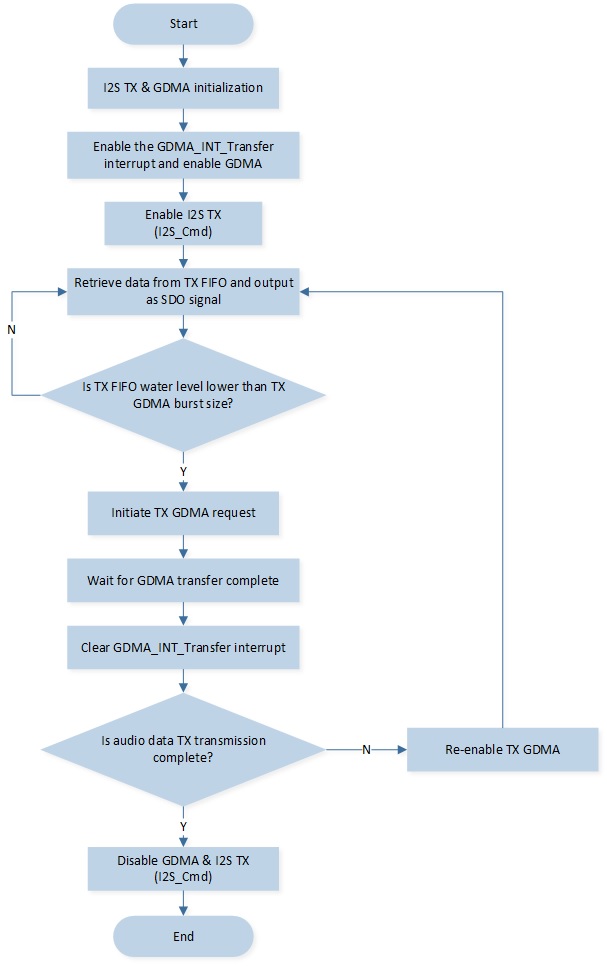
I2S RX GDMA Handshake Operation
Turn on the peripheral clock source of the GDMA.
I2S RX and GDMA initialization: Set GDMA handshake with I2S RX.
Enable the
GDMA_INT_Transferinterrupt and enable GDMA.Invoke
I2S_Cmdto generate LRCK and start sending data to RX FIFO.Wait for RX FIFO data to exceed RX GDMA burst size and initiate GDMA request.
Trigger GDMA transfer interrupt and wait for GDMA transfer to complete.
Clear
GDMA_INT_Transferinterrupt.
The flow chart of I2S RX GDMA handshake operation is shown in the following figure.

The codes below demonstrate the I2S GDMA handshake initialization flow.
void driver_gdma_init(T_I2S_CONFIG_DIR dir)
{
    GDMA_InitTypeDef gdma_init;
    NVIC_InitTypeDef nvic_init;

    RCC_PeriphClockCmd(APBPeriph_GDMA, APBPeriph_GDMA_CLOCK, ENABLE);

    GDMA_StructInit(&gdma_init);
    gdma_init.GDMA_BufferSize           = I2S_DMA_BUF_LEN;
    gdma_init.GDMA_SourceDataSize       = GDMA_DataSize_Word;
    gdma_init.GDMA_DestinationDataSize  = GDMA_DataSize_Word;
    gdma_init.GDMA_SourceMsize          = GDMA_Msize_4;
    gdma_init.GDMA_DestinationMsize     = GDMA_Msize_4;

    if (dir == I2S_CONFIG_TX)
    {
        gdma_init.GDMA_ChannelNum           = I2S_TX_DMA_CHANNEL_NUM;
        gdma_init.GDMA_DIR                  = GDMA_DIR_MemoryToPeripheral;
        gdma_init.GDMA_SourceAddr           = (uint32_t)(i2s_send_buff);
        gdma_init.GDMA_DestinationAddr      = (uint32_t)I2S_TX_ADDR;
        gdma_init.GDMA_SourceInc            = DMA_SourceInc_Inc;
        gdma_init.GDMA_DestinationInc       = DMA_DestinationInc_Fix;
        gdma_init.GDMA_DestHandshake        = I2S_TX_DMA_HANDSHAKE;
        GDMA_Init(I2S_TX_DMA_CHANNEL, &gdma_init);

        RamVectorTableUpdate(I2S_TX_DMA_VECTOR, i2s_tx_dma_handler);

        nvic_init.NVIC_IRQChannel           = I2S_TX_DMA_IRQ;
    }
    else if (dir == I2S_CONFIG_RX)
    {
        gdma_init.GDMA_ChannelNum           = I2S_RX_DMA_CHANNEL_NUM;
        gdma_init.GDMA_DIR                  = GDMA_DIR_PeripheralToMemory;
        gdma_init.GDMA_SourceAddr           = (uint32_t)I2S_RX_ADDR;
        gdma_init.GDMA_DestinationAddr      = (uint32_t)(i2s_recv_buff);
        gdma_init.GDMA_SourceInc            = DMA_SourceInc_Fix;
        gdma_init.GDMA_DestinationInc       = DMA_DestinationInc_Inc;
        gdma_init.GDMA_SourceHandshake      = I2S_RX_DMA_HANDSHAKE;
        GDMA_Init(I2S_RX_DMA_CHANNEL, &gdma_init);

        RamVectorTableUpdate(I2S_RX_DMA_VECTOR, i2s_rx_dma_handler);

        nvic_init.NVIC_IRQChannel           = I2S_RX_DMA_IRQ;
    }

    nvic_init.NVIC_IRQChannelCmd        = (FunctionalState)ENABLE;
    nvic_init.NVIC_IRQChannelPriority   = 3;
    NVIC_Init(&nvic_init);
}
SDIO
SDIO Demo Code Support List
Demo 1 |
sdio_demo.c |
|---|---|
Sample Purpose |
Demonstrates how PC communicates with SD card. |
Brief Introduction |
This sample code demonstrates SD card read and write function. Read the data at the specified address of the SD card, and write the specified data to the SD card. |
File Path |
|
Function Entry |
|
Supply Voltage |
3.3V, check rcfg of Voltage Setting. |
Group Pins |
The specific group pins are shown in SDIO Group Pins in RTL87x3D and SDIO Group Pins in RTL87x3E. |
Hardware Connection |
Take RTL87x3D Group0 as an example, shown in SDIO Hardware Connection Diagram. The 6 pins of the SD card are respectively connected with Group0 on EVB, and the VDD and GND pins of the SD card are connected with the VCC and GND pins on EVB. |
Expected Result |
Press the reset button on the EVB, the string ‘sd_print_binary_data: buf:’ will be printed in Debug Analyzer. The last printed data buf is 0~FF+0~FF (512 bytes). |
Demo 2 |
sdio_fs_demo.c |
|---|---|
Sample Purpose |
Demonstrates how PC communicates with SD card by filesystem. |
Brief Introduction |
This sample code demonstrates SD card read and write function by filesystem. FatFS_DirectoyDemo can write the data under the specified directory file of the SD card; FatFS_Demo can write and read data directly to the SD card file. |
File Path |
|
Function Entry |
|
Supply Voltage |
3.3V, check rcfg of Voltage Setting. |
Group Pins |
The specific group pins are shown in SDIO Group Pins in RTL87x3D and SDIO Group Pins in RTL87x3E. |
Hardware Connection |
Take RTL87x3D Group0 as an example, shown in SDIO Hardware Connection Diagram. The 6 pins of the SD card are respectively connected with Group0 on EVB, and the VDD and GND pins of the SD card are connected with the VCC and GND pins on EVB. |
File Prepare |
1. FatFS_DirectoyDemo: The BBpro directory and written files need to be created in the root directory. |
Expected Result |
1. Press the reset button on the EVB. |
Demo 3 |
sdio_card_detect_demo.c |
|---|---|
Sample Purpose |
Demonstrates SD card detection by GPIO. |
Brief Introduction |
This sample code demonstrates the SD card detection function. Simulate SD card insertion and removal through GPIO. |
File Path |
|
Function Entry |
|
Supply Voltage |
3.3V, check rcfg of Voltage Setting. |
Selected CD Pin Definition |
|
Group Pins |
The specific group pins are shown in SDIO Group Pins in RTL87x3D and SDIO Group Pins in RTL87x3E. |
Hardware Connection |
Take RTL87x3D Group0 as an example, shown in SDIO Hardware Connection Diagram. The 6 pins of the SD card are respectively connected with Group0 on EVB, and the VDD and GND pins of the SD card are connected with the VCC and GND pins on EVB. |
Expected Result |
Connect P0_3 with GND on EVB, the string ‘gpio_isr_cb: card insert!’ will be printed in Debug Analyzer. Remove P0_3 from GND, the string ‘gpio_isr_cb: card remove!’ will be printed in Debug Analyzer. |
RTL87x3D |
CLK |
CMD |
DAT0 |
DAT1 |
DAT2 |
DAT3 |
|---|---|---|---|---|---|---|
Group0 pins |
P1_2 |
P1_3 |
P1_4 |
P1_5 |
P1_6 |
P1_7 |
Group1 pins |
P4_2 |
P4_3 |
P4_4 |
P4_5 |
P4_6 |
P4_7 |
RTL87x3E |
CLK |
CMD |
DAT0 |
DAT1 |
DAT2 |
DAT3 |
|---|---|---|---|---|---|---|
Group0 pins |
P5_0 |
P5_1 |
P5_2 |
P5_3 |
P5_4 |
P5_5 |
Group1 pins |
P6_0 |
P6_1 |
P6_2 |
P6_3 |
P6_4 |
P6_5 |
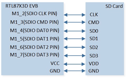
Function Description
SDIO
Secure Digital Input and Output, defines a peripheral interface. SDIO card is an IO device that uses the SD bus and SD commands. The shape and interface of the SDIO card are compatible with the SD card, but it not only realizes the storage function, but also realizes other functions, such as Bluetooth, Wireless Fidelity, etc.
SDHC
SD host controller, the connection of SDHC and SD card is shown in SDHC and SD Card Connection Diagram. The host controls the internal operation of the SD card by reading/writing SDHC internal registers.
SDIO transmission mode
SPI mode, 1-bit mode (single-wire), 4-bit SD mode (four-wire). The pin definitions in different modes are shown in SDIO Pin Definitions in Different Modes.
SDIO interface definition (4-bit SD mode)
CLK
Host to card clock signal.
CMD
Bi-directional command/response signal.
DAT0-DAT3
4 Bi-directional data signals.
Note
RTL87x3D, RTL87x3E, and RTL87x3EP support SDIO.
Pins |
4-Bit Mode |
1-Bit Mode |
SPI mode |
|---|---|---|---|
1 |
VCC |
VCC |
VCC |
2 |
VSS1 |
VSS1 |
VSS1 |
3 |
VSS2 |
VSS2 |
VSS2 |
4 |
CLK |
CLK |
CLK |
5 |
CMD |
CMD |
CS |
6 |
DAT0 |
DAT0 |
DAT0 |
7 |
DAT1 |
RSV |
DAT1 |
8 |
DAT2 |
RSV |
RSV |
9 |
DAT3/CD |
CD |
RSV |
Feature List
Support SD Spec V2.0.
Support only 2 Group Pins on EVB to communicate with SD card. For specific pins, please refer to SDIO Group Pins in RTL87x3D or SDIO Group Pins in RTL87x3E.
Support 1-bit and 4-bit SD bus width.
Support optional bus clock, 40MHz and 80MHz can only support in RTL87x3D.
Support multiple block and single block transfer, SDHC max block size is 512 Bytes.
High Voltage SD card: operation Voltage 3.3V.
Support DMA transfer.
Support interrupt control.
SD Bus Protocol
The control on the SD bus is realized through CMD: The host initiates a request, and then the SD card responds to the request.
Data transfer format: Start bit 0, first MSB, then LSB, CRC check, end bit 1.
Data is transferred in the form of data blocks. SD Bus block read and write operation, as shown in SD BUS (Multiple) Block Read Operation and SD BUS (Multiple) Block Write Operation.
Take the SD Bus multi-block read operation as an example:
The host sends a multi-block read command.
The SD card sends a response.
The card starts sending data.
After each block is sent, return a CRC status.
The card transmits the next block data.
Until the host sends a stop command, the card responds.
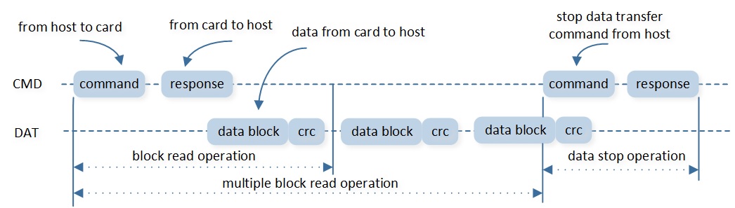
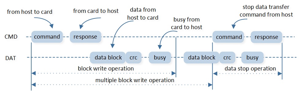
SDIO Operation Flow
The codes below demonstrate the SD card initialization flow.
const T_SD_CONFIG    sd_card_cfg =
{
    .sd_if_type = SD_IF_SD_CARD,
    .sdh_group = GROUP_0,
    .sdh_bus_width = SD_BUS_WIDTH_4B,
    .sd_bus_clk_sel = SD_BUS_CLK_20M
};

/* SD config init */
sd_config_init((T_SD_CONFIG *)&sd_card_cfg);
/* Group pins PINMUX & PAD Config */
sd_board_init();
/* Initialize SD card peripheral */
sd_card_init();
The codes below demonstrate the SD card communication flow. For details, please refer to src\sample\io_demo\sdio\sdcard\sdio_demo.c.
static uint8_t *test_buf = NULL;
uint32_t sd_status = 0;

void sd_test(void)
{
    memset(test_buf, 0, sizeof(test_buf));
    /* Read the data at the specified address of the SD card */
    sd_status = sd_read(OPER_SD_CARD_ADDR, (uint32_t)test_buf, SINGLE_BLOCK_SIZE, BLOCK_NUM);

    if (sd_status != 0)
    {
        return ;
    }
    /*SD card print the binary data of test_buf */
    sd_print_binary_data(test_buf, SINGLE_BLOCK_SIZE * BLOCK_NUM);

    for (uint32_t i = 0; i < SINGLE_BLOCK_SIZE * BLOCK_NUM; i++)
    {
        test_buf[i] = i & 0xff;
    }
    sd_print_binary_data(test_buf, SINGLE_BLOCK_SIZE * BLOCK_NUM);
    /* Write the specified test_buf data to the SD card */
    sd_status = sd_write(OPER_SD_CARD_ADDR, (uint32_t)test_buf, SINGLE_BLOCK_SIZE, BLOCK_NUM);
}
The codes below demonstrate the SD card communication flow by filesystem.
For details, please refer to src\sample\io_demo\sdio\sdcard\demo\sdio_fs_demo.c.
void FatFS_Demo(void)
{
    uint32_t a = 1;
    uint32_t res = 0;
    const char driver_num = 0;

    /* Create workspace */
    res = f_mount(&fs, &driver_num, 1);

    /* Open file */
    res = f_open(&fdst, "Test.txt", FA_CREATE_ALWAYS | FA_WRITE);
    if (res != FR_OK)
    {
        //Open file failure, add error handle code here
        f_close(&fdst);
        return ;
    }

    res = f_open(&fsrc, "Data.txt", FA_OPEN_EXISTING | FA_READ);
    if (res != FR_OK)
    {
        //Open file failure, add error handle code here
        f_close(&fsrc);
        return ;
    }

    /* File operation */
    for (uint32_t i = 0; i < 1024; i++)
    {
        buffer[i] = i % 0x09 + 0x30;
    }
    buffer[1021] = 69;
    buffer[1022] = 69;
    buffer[1023] = 69;
    f_write(&fdst, buffer, 1024, &a);

    memset(buffer, 0, 1024);
    f_read(&fsrc, buffer, 1024, &a);

    /* Close file */
    f_close(&fsrc);
    f_close(&fdst);
}