One Shot Interrupt
This sample demonstrates voltage detection using the ADC single-sample interrupt mode.
When the ADC sampling is complete, an interrupt is triggered, and within the interrupt function, raw data is read and voltage conversion calculations are performed.
Users can change the sampling mode of the ADC channel, input voltage range, and other information in the sample through different macro configurations. For specific macro configurations, see Configurations.
Requirements
For requirements, please refer to the Requirements.
Wiring
Use a Dupont wire to connect P2_4 to external voltage input.
Configurations
-
The following macro can be configured to modify whether the ADC sample value is stored in the FIFO.
1indicates that the ADC sample data is stored in the FIFO, while0indicates that the ADC data is stored in the corresponding Schedule Table.#define ADC_DATA_OUTPUT_TO_FIFO 0 /*< Set this macro to configure whether ADC data is stored in the FIFO. */
-
The following macro can be configured to modify the pin definitions.
#define ADC_DIVIDE_MODE                     1                   /*< Divide Mode, input voltage range is 0V~Vbat. */
#define ADC_BYPASS_MODE                     0                   /*< Bypass Mode, input voltage range is 0V~0.9V. */

#define ADC_MODE_DIVIDE_OR_BYPASS           ADC_DIVIDE_MODE     /*< Set this macro to select the ADC input voltage range. */
-
The following macros can be configured to modify the pin definitions.
#define ADC_SAMPLE_PIN                      P2_4
#define ADC_SAMPLE_CHANNEL                  ADC_Channel_Index_4
Building and Downloading
For building and downloading, please refer to the Building and Downloading.
Experimental Verification
-
When the EVB starts, observe the following log within the Debug Analyzer
Start ADC interrupt test!
-
ADC Configurations:
-
If
ADC_MODE_DIVIDE_OR_BYPASSis configured asADC_DIVIDE_MODE, the following log will be printed:[ADC]ADC sample mode is divide mode !
-
If
ADC_MODE_DIVIDE_OR_BYPASSis configured asADC_BYPASS_MODE, the following log will be printed:[ADC]ADC sample mode is bypass mode !
-
-
After initialization is completed, the ADC begins sampling. Once a single ADC sampling is finished, it will trigger an interrupt, within which the raw data obtained from sampling and the converted voltage value will be printed.
into SAR_ADC_Handler
[ADC] adc_sample_demo: ADC one shot mode sample data = xxx, voltage = xxx mV
...
Code Overview
This section introduces the code and process description for initialization and corresponding function implementation in the sample.
Source Code Directory
The directory for project file and source code are as follows:
Project directory:
sdk\samples\peripheral\adc\oneshot_interrupt\projSource code directory:
sdk\samples\peripheral\adc\oneshot_interrupt\src
Initialization
The initialization flow for peripherals can refer to Initialization Flow in General Introduction.
-
Call
Pad_Config()andPinmux_Config()to configure the PAD and PINMUX of the corresponding pins. Please ensure that the PAD is configured in Shutdown mode to prevent leakage.void board_adc_init(void) { Pad_Config(ADC_SAMPLE_PIN, PAD_SW_MODE, PAD_NOT_PWRON, PAD_PULL_NONE, PAD_OUT_DISABLE, PAD_OUT_LOW); }
Call
RCC_PeriphClockCmd()to enable the ADC clock.-
Initialize the ADC peripheral:
Define the
ADC_InitTypeDeftypeADC_InitStruct, and callADC_StructInit()to pre-fillADC_InitStructwith default values.Modify the
ADC_InitStructparameters as needed. WhenADC_DATA_OUTPUT_TO_FIFOis configured with different values, the initialization configuration will be different. The ADC initialization parameter configuration is shown in the table below.Call
ADC_Init()to initialize the ADC peripheral.
ADC Hardware Parameters |
Setting in the |
|
|
|---|---|---|---|
Sample Time |
255 |
255 |
|
Schedule Index |
Index 0 is set to |
Index 0 is set to |
|
Bit Map |
0x01 |
0x01 |
|
Data Write to FIFO |
|||
FIFO Threshold Level |
- |
0x0A |
|
Power Always On |
If
ADC_MODE_DIVIDE_OR_BYPASSis configured asADC_BYPASS_MODE, the functionADC_BypassCmd()must be called to enable the Bypass mode for the corresponding pin.-
Call
ADC_INTConfig()to configure the ADC interrupt and NVIC. For NVIC configurations, refer to Interrupt Configuration.If
ADC_DATA_OUTPUT_TO_FIFOis configured as0, configure the ADC one shot done interruptADC_INT_ONE_SHOT_DONE.If
ADC_DATA_OUTPUT_TO_FIFOis configured as1, configure the ADC FIFO threshold interruptADC_INT_FIFO_THD.
Before the ADC begins sampling, it is necessary to call
ADC_CalibrationInit()for ADC voltage calibration. If the return value is false, it indicates that the IC has not been calibrated and cannot accurately convert voltage values, but raw data can still be read.
Functional Implementation
ADC Sampling Data Not Stored in FIFO
When ADC sampling data is not stored in FIFO, the flow of one shot interrupt mode is shown in the figure:
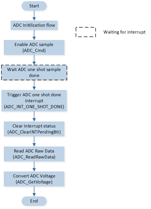
ADC one shot interrupt mode flow (ADC Sampling Data Not Stored in FIFO)
Loop call
ADC_Cmd()to start ADC sampling.-
When ADC sampling is complete, trigger the ADC one shot done interrupt
ADC_INT_ONE_SHOT_DONE. Within the interrupt function, call theADC_ReadRawData()function to read the sampling data of the corresponding channel. Execute theADC_GetVoltage()function, input the corresponding sampling mode, and convert the sampling data to a voltage value.void SAR_ADC_Handler(void) { DBG_DIRECT("into SAR_ADC_Handler"); ADC_ErrorStatus error_status = NO_ERROR; #if (!ADC_DATA_OUTPUT_TO_FIFO) ... if (ADC_GetINTStatus(ADC, ADC_INT_ONE_SHOT_DONE) == SET) { ADC_ClearINTPendingBit(ADC, ADC_INT_ONE_SHOT_DONE); sample_data = ADC_ReadRawData(ADC, ADC_Schedule_Index_0); #if (ADC_MODE_DIVIDE_OR_BYPASS == ADC_BYPASS_MODE) sample_voltage = ADC_GetVoltage(BYPASS_SINGLE_MODE, (int32_t)sample_data, &error_status); #else sample_voltage = ADC_GetVoltage(DIVIDE_SINGLE_MODE, (int32_t)sample_data, &error_status); #endif ... } #else ... #endif }
ADC Sampling Data Stored in FIFO
When ADC sampling data is stored in FIFO, the flow of one shot interrupt mode is as shown in the figure:
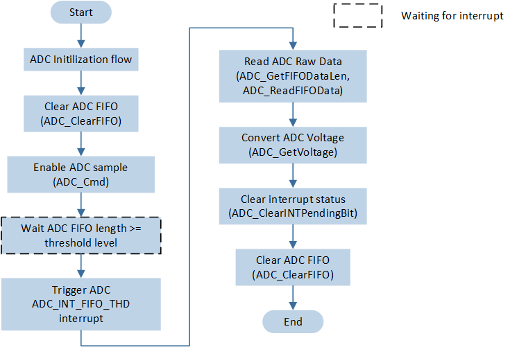
ADC one shot interrupt mode flow (ADC Sampling Data Stored in FIFO)
Before ADC sampling, call
ADC_ClearFIFO()to clear the data in the ADC FIFO.Loop call
ADC_Cmd()to start ADC sampling.When the sampled data in the FIFO reaches the threshold, trigger the ADC
ADC_INT_FIFO_THDinterrupt, and within the interrupt function, callADC_GetFIFODataLen()to read the data length in the FIFO; callADC_ReadFIFOData()function to read the data in the FIFO; callADC_GetVoltage()function, input the corresponding sampling mode, and convert the sampled data to voltage values.-
After the data processing is complete, call
ADC_ClearFIFO()to clear the data in the ADC FIFO.void SAR_ADC_Handler(void) { DBG_DIRECT("into SAR_ADC_Handler"); ADC_ErrorStatus error_status = NO_ERROR; #if (!ADC_DATA_OUTPUT_TO_FIFO) ... #else if (ADC_GetINTStatus(ADC, ADC_INT_FIFO_THD) == SET) { uint16_t data_len = ADC_GetFIFODataLen(ADC); ADC_ReadFIFOData(ADC, sample_data, data_len); for (uint8_t i = 0; i < data_len; i++) { #if (ADC_MODE_DIVIDE_OR_BYPASS == ADC_BYPASS_MODE) sample_voltage[i] = ADC_GetVoltage(BYPASS_SINGLE_MODE, (int32_t)sample_data[i], &error_status); #else sample_voltage[i] = ADC_GetVoltage(DIVIDE_SINGLE_MODE, (int32_t)sample_data[i], &error_status); #endif ... } ADC_ClearINTPendingBit(ADC, ADC_INT_FIFO_THD); ADC_ClearFIFO(ADC); } #endif }
See Also
Please refer to the relevant API Reference: