Flash
Flash is non-volatile storage. Compared to RAM, which can be written or read directly, Flash must be emptied or erased before being written. Flash supports at least 100K Program-Erase cycles. It can also develop bad blocks when the same blocks are erased frequently.
This document guides on how to use Flash, covering the following topics:
-
Flash Basic Operations
Introduction to Flash API.
-
Flash Section
Help users place data/functions in different areas.
-
Flash Translation Layer
Introduction on how to use the FTL, which is designed for lightweight dynamic parameter storage.
-
External Flash
Introduces the external Flash from the architecture perspective to the application level.
It is recommended to use the FTL rather than the Flash driver for user data storage.
If it is really needed to operate Flash directly, APIs with the fmc_ prefix can be used.
External Flash is supported. Multiple choices are available for basic functions like single-mode read, write, and erase. However, the Flash driver also provides some advanced functions such as quad mode, deep power-down, and Flash block protection. Not all Flash supports these functions, so if needed, Realtek can provide an Approved Vendor List.
Basic Operations
Flash provides a set of interfaces in sdk\inc\hal\platform\fmc_api.h.
This chapter introduces the standard functions: read, write, and erase.
Flash ensures task safety for these functions. This means that all Flash basic operations cannot be executed at the same time. That's because there is only one resource (Flash) and only one path (Flash controller) to access it. This helps prevent multiple tasks or interrupts from destroying the atomicity of the SPIC command sequence.
Read
Function |
|
|---|---|
Prototype |
|
Description |
Read Flash data. |
Instruction |
This function reads data from the Flash in user mode. |
Auto DMA Read
Function |
|
|---|---|
Prototype |
|
Description |
Read Flash data by DMA. |
Instruction |
This function reads data from the Flash in auto mode by DMA. |
If users need to read a large amount of data (such as 1K Bytes), this API is recommended. DMA read is faster than fmc_flash_nor_read().
Write
Function |
|
|---|---|
Prototype |
|
Description |
Write data to Flash. |
Instruction |
This function writes data to the Flash in user mode. |
This function modifies the Flash data through SPIC rather than the bus command, so this operation will not affect the data in the Cache.
In this case, auto read will return the old data in the Cache. Users can flush the Cache or use fmc_flash_nor_read() to get the correct data after running fmc_flash_nor_write().
Erase
Function |
|
|---|---|
Prototype |
|
Description |
Erase Flash. |
Instruction |
Users should call Flash erase before write. |
This function supports three erase modes:
FMC_FLASH_NOR_ERASE_CHIP: Erase whole chip.FMC_FLASH_NOR_ERASE_SECTOR: Erase 4K Bytes. The input address must be 4K aligned.FMC_FLASH_NOR_ERASE_BLOCK: Erase 64K Bytes. The input address must be 64K aligned.
Section Usage
Functions are placed on Flash by default. Sections are provided for users to move them to the RAM area. See sdk\inc\platform\section.h.
#define FLASH_HEADER     __attribute__((section(".flash.header")))     __attribute__((used))
#define FLASH_HEADER_EXT __attribute__((section(".flash.header_ext"))) __attribute__((used))
#define RAM_TEXT_SECTION __attribute__((section(".ram_text")))
#define SHM_DATA_SECTION __attribute__((section(".shm.data")))
#define ISR_TEXT_SECTION __attribute__((section(".isr.text"))) /*not very urgent isr*/
-
FLASH_HEADER&FLASH_HEADER_EXTThis two sections are provided for the image header.
FLASH_HEADER const T_IMG_HEADER_FORMAT img_header =
{
    ...
}
-
RAM_TEXT_SECTIONFunctions with this section prefix will be placed in RAM.
RAM_TEXT_SECTION bool app_io_msg_send(T_IO_MSG *io_msg)
{
    T_EVENT_TYPE event = EVENT_IO_TO_APP;
    bool ret = false;

    if (os_msg_send(audio_io_queue_handle, io_msg, 0) == true)
    {
        ret = os_msg_send(audio_evt_queue_handle, &event, 0);
    }

    if (ret == false)
    {
        APP_PRINT_ERROR3("app_io_msg_send failed, type = %x, subtype = %x, param = %x",
                         io_msg->type, io_msg->subtype, io_msg->u.param);
    }

    return ret;
}
-
SHM_DATA_SECTIONFunctions with this section prefix will be placed in DSP share memory. Please make sure DSP share memory is ready first.
SHM_DATA_SECTION uint8_t name_buf[NAME_BUF_SIZE];
-
ISR_TEXT_SECTIONISR functions need to be placed in RAM because if the Flash is being erased, XIP would fail to execute properly, leading to a hard fault.
This section is provided for users to run XIP in ISR. However, there is a limitation: users must ensure that the ISR handler includes this prefix.
static ISR_TEXT_SECTION void GPIOA0_Handler(void)
{
    imp_gpio_handler(GPIOA, 0, BIT0, hal_gpio_sw_context.gpio_a0_callback);
}

static ISR_TEXT_SECTION void imp_gpio_handler(GPIO_TypeDef *GPIOx, uint8_t gpio_num, uint32_t gpio_pin, P_GPIO_CBACK callback)
{
    GPIOx_ClearINTPendingBit(GPIOx, gpio_pin);
    if (callback)
    {
        callback(hal_gpio_sw_context.context[gpio_num]);
    }
    else
    {
        IO_PRINT_ERROR1("empty isr callback for gpioa%u", gpio_num);
    }
}
If the RAM is enough, users could put this section to RAM in the .sct file without modifying any code.
Put functions with this section prefix on Flash:
      FLASH_TEXT +0;
      {
          startup_rtl87x3e.o (RESET, +First)
#if (FEATURE_RAM_CODE == 0)
          * (+RO)
#endif
          * (.isr.text)
      }
Move functions with
ISR_TEXT_SECTIONprefix to RAM:RAM_TEXT APP_BUFFER_ON_ADR APP_BUFFER_ON_SIZE { #if FEATURE_RAM_CODE .ANY (+RO) #endif * (.ram_text) * (.isr.text) }
Flash Transport Layer
Flash Transport Layer is used as an abstraction layer for users to read & write data on Flash.
The location of FTL POOL in Flash can be found in flash_map.h.
The purpose of FTL is to make it simpler to change the data stored in Flash:
Traditionally, each time users want to change data on Flash, the Flash needs to be erased first. If Flash is modified frequently, a lot of time will be wasted on erasing. FTL replaces the physical address with the logical address to access Flash. FTL records data and its logical address on Flash. If a user wants to modify the data, FTL writes a new record rather than modifying the old record. In this way, users do not need to erase Flash. When the FTL detects that there is not enough space to write a new record, it will clear some expired records. This process is called Garbage Collection.
Since FTL is designed for lightweight dynamic parameter storage, heavyweight and read-only data should not use it.
FTL uses modules to distinguish different data. FTL has a default module to ensure basic functionality. Users can save data in the default module, or apply for a new module.
Default FTL Module
The data in the default module can be divided into the following regions. FTL layout is shown in the following figure:
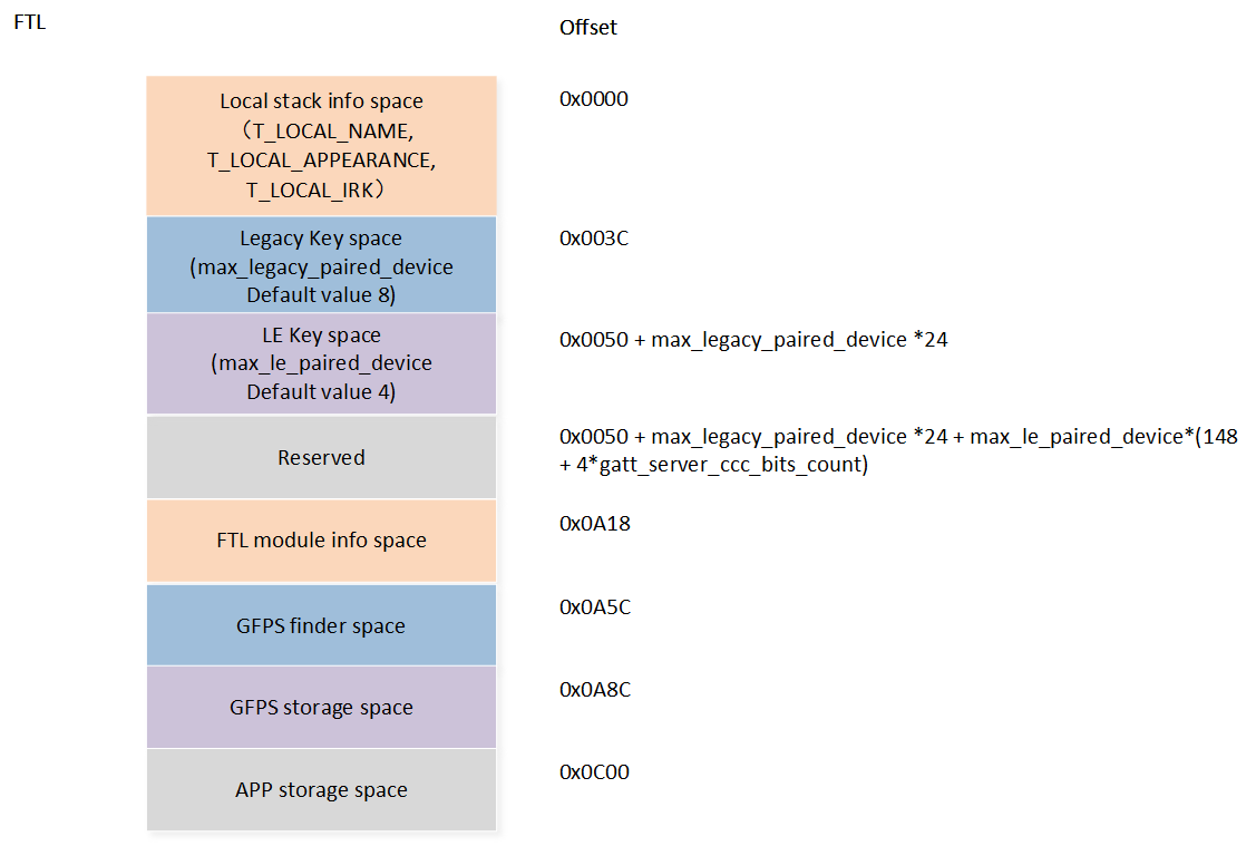
FTL Layout
-
Local Stack Information Space
This region is used to store local stack information including device name, device appearance, and lock IRK.
-
Legacy Key Space
This region is used to store legacy key information. The size of this region can be configured by MCUConfig Tool.
-
LE Key Space
This region is used to store LE key information. The size of this region can be configured by MCUConfig Tool.
-
Reserved
This region is reserved space. Because the variables
max_legacy_paired_deviceandmax_le_paired_deviceare configurable, this region can be used to expand Legacy key storage space and LE key storage space. When variablesmax_legacy_paired_deviceandmax_le_paired_deviceare determined, this region can be used by APP. -
FTL Module Information Space
This region records the FTL EXT module's information.
-
GFPS Finder Space
This region can be used by APP to store GFPS Finder information.
-
GFPS Storage Space
This region can be used by APP to store GFPS information.
-
APP Storage Space
This region can be used by APP to store information.
The maximum size of the default module should be set by the interface: ftl_set_rom_module_size().
An easy way to calculate the Flash area size is logical_size * 2.
FTL uses a mapping table to save time, and the default FTL module takes nearly logical_size / 2 SRAM.
FTL APIs of Default FTL Module
Default FTL APIs could be found in sdk\inc\hal\platform\ftl.h.
Read
Function |
|
|---|---|
Prototype |
|
Description |
Read data from the default FTL module. |
Instruction |
The offset that can be used by the APP starts from 0x0C00 and must be 4 Bytes aligned. |
Write
Function |
|
|---|---|
Prototype |
|
Description |
Write data to the default FTL module. |
Instruction |
The offset that can be used by the APP starts from 0x0C00 and must be 4 Bytes aligned. |
A brief demo:
static void app_cfg_load(void)
{
    ...
    if (app_cfg_nv.hdr.sync_word != DATA_SYNC_WORD)
    {
        // Load factory reset bit first when MPPG Tool factory reset
        if (app_cfg_nv.hdr.length == 0)
        {
            ftl_load_from_storage(&app_cfg_nv.eq_idx_anc_mode_record, APP_RW_DATA_ADDR + FACTORY_RESET_OFFSET,
                                  4);
        }


       app_cfg_reset();
    }
    ...
}

uint32_t app_cfg_store(void *pdata, uint16_t size)
{
...

   return ftl_save_to_storage(pdata, offset + APP_RW_DATA_ADDR, size);
}
Add an FTL Module
FTL POOL supports up to 7 modules. The default FTL module takes up one.
FTL module APIs are provided in sdk\inc\hal\platform\ftl.h.
Create an FTL Module
Function |
|
|---|---|
Prototype |
|
Description |
Create an FTL module. |
Instruction |
The |
Before adding a new FTL module, please ensure that the Flash size of the FTL POOL is sufficient. Refer to Estimate the Min Flash Size of FTL POOL.
If ((block_len + 4) % 8) == 0, the new module will occupy malloc_size / block_len * (block_len + 4) Flash area.
Otherwise, it will occupy malloc_size / block_len * (block_len + 8) Flash area. The mapping table for this new FTL module will occupy malloc_size / block_len * 2 SRAM.
Note
The first 4 Bytes of module_name should be unique.
Read
Function |
|
|---|---|
Prototype |
|
Description |
Read data from an FTL module. |
Instruction |
The offset that can be used starts from 0. |
Write
Function |
|
|---|---|
Prototype |
|
Description |
Write data to an FTL module. |
Instruction |
The offset that can be used starts from 0. |
The block_len in ftl_init_module() is the smallest unit for reading and writing data in the current FTL module.
Applications may need additional operations on the read/write data if necessary.
Demo:
#define EQ_EXT_FTL_PARTITION_NAME "EQ_FTL"
#define EQ_SIZE     (0x2800)
#define EQ_EXT_FTL_BLOCK_LEN     68

int32_t eq_ext_ftl_partition_init(const T_STORAGE_PARTITION_INFO *info)
{
    return ftl_init_module(EQ_EXT_FTL_PARTITION_NAME, EQ_SIZE, EQ_EXT_FTL_BLOCK_LEN);
}

int32_t eq_ext_ftl_partition_write(const T_STORAGE_PARTITION_INFO *info, uint32_t offset,
                                   uint32_t len, void *buf)
{
    return ftl_save_to_module(EQ_EXT_FTL_PARTITION_NAME, (void *)buf, offset, len);
}

int32_t eq_ext_ftl_partition_read(const T_STORAGE_PARTITION_INFO *info, uint32_t offset,
                                  uint32_t len, void *buf)
{
     return ftl_load_from_module(EQ_EXT_FTL_PARTITION_NAME, (void *)buf, offset, len);
}

void eq_ext_ftl_storage_init(void)
{
    static const T_STORAGE_PARTITION_INFO eq_partitions[] =
    {
        {
            .name = EQ_EXT_FTL_PARTITION_NAME,
            .address = NULL,
            .size = NULL,
            .perm = STORAGE_PERMISSION_READ | STORAGE_PERMISSION_WRITE,
            .media_type = STORAGE_MEDIA_TYPE_NOR,
            .content_type = STORAGE_CONTENT_TYPE_RW_DATA,
            .init = eq_ext_ftl_partition_init,
            .read = eq_ext_ftl_partition_read,
            .write = eq_ext_ftl_partition_write,
            .erase = NULL,
            .async_read = NULL,
            .async_write = NULL,
            .async_erase = NULL,
        },
    };

    storage_partition_init(eq_partitions, sizeof(eq_partitions) / sizeof(eq_partitions[0]));
}
FTL POOL
All FTL modules save data in the same Flash area (FTL POOL), which can be found in flash_map.h. Users can modify it directly, or use the Flash Map Generate Tool.
So the address and size of the FTL POOL are determined by APP and cannot be modified by any other bins or tools.
In principle, the new FTL POOL must include all areas of the old FTL POOL. In principle, the new FTL POOL must include all areas of the old FTL POOL. Otherwise, FTL data would be lost. In these conditions, users need to do a Factory Reset.
#define FTL_ADDR                        0x021F9000
#define FTL_SIZE                        0x00007000  // 28K Bytes
Estimate the Min Flash Size of FTL POOL
-
Garbage Collection
Use 8K to do GC.
-
Default FTL Module
Takes up
logical_size * 2Flash area. -
EXT FTL Module
Takes up
logical_size / block_len * (block_len + (block_len % 8) ? 8 : 4)Flash area.
The size of the FTL POOL should be larger than the total size above, must be 4K aligned.
FTL Cache
FTL has a cache that is on the heap. Users can enable the FTL cache by the interface ftl_cache_init().
The parameter in ftl_cache_init() specifies the size of the FTL cache and is recommended to be set to at least 128 Bytes.
example:
ftl_cache_init(128);
After enabling FTL cache, FTL saves data in the FTL cache area when there is not enough space to write a new record.
-
Advantages:
Reduces current write's time cost.
If there is no space for a new record, FTL needs to execute GC. GC calls Flash write & erase operation, this costs at least 50ms+. So if the current flow is time sensitive, it is suggested to enable FTL cache.
-
Disadvantages:
Data loss in an abnormal case.
Because data is in the FTL cache, not on Flash, it will be lost if power is lost or an abnormal reboot happens.
External Flash
Besides the MCM Flash embedded in the SoC, some Realtek Bluetooth SoCs support additional external Flash if the desired Flash size is larger than the embedded one. Please contact Realtek to check whether specific IC supports it.
The chapter will take RTL8773D as an example to introduce it from the architecture perspective to the application level when the SDK user wants to add more Flashes into the system.
Note
The material in this chapter is captured from the latest RTL8773D document for external customers, but this may be subject to change. So please refer to the latest ones in case any changes are made.
System Architecture
The system architecture of RTL87x3D is shown in the following figure.
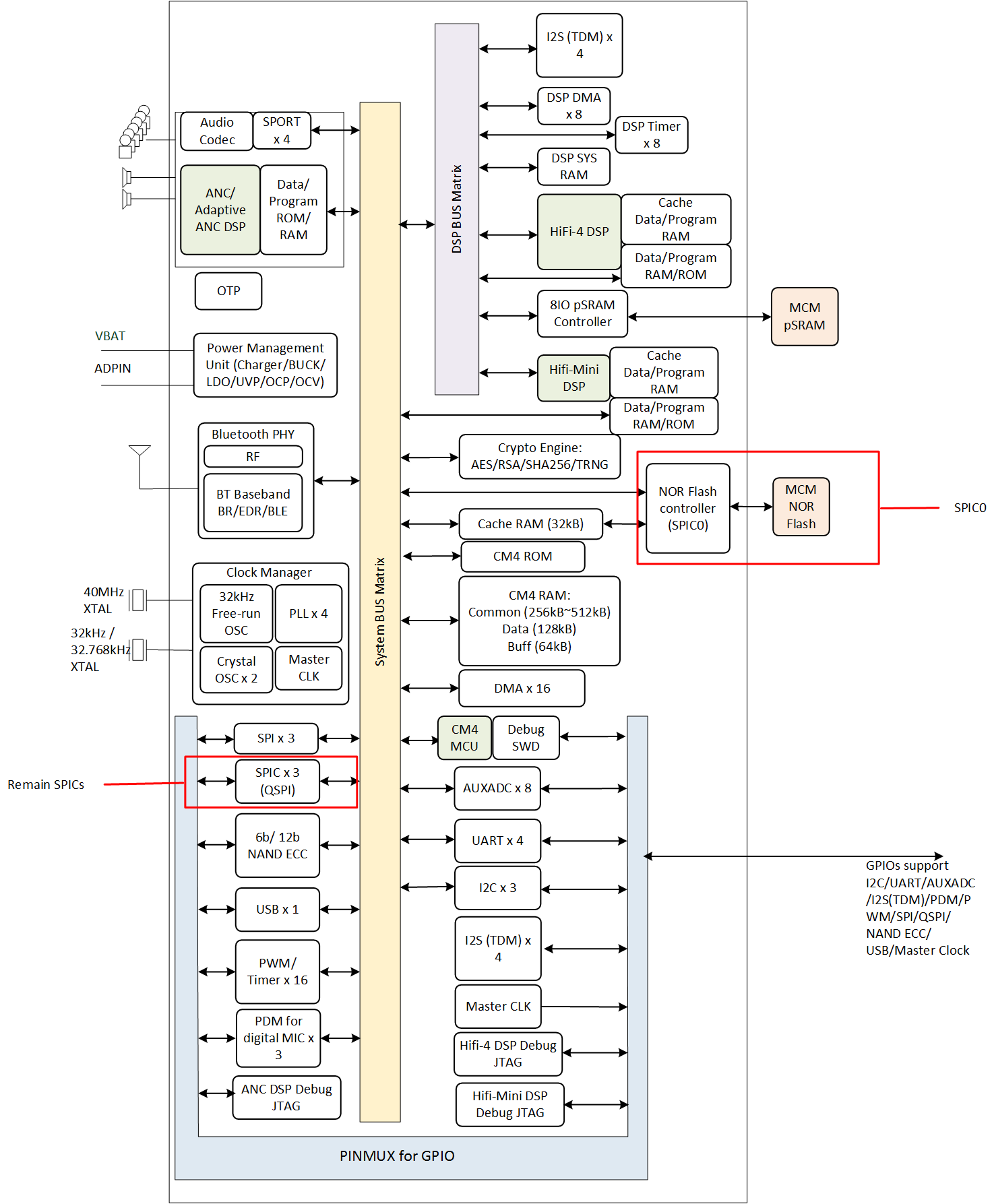
System Architecture of RTL87x3D
The picture above is captured from the system overview of RTL8773D in the data sheet, and it clearly shows that SPIC0 is reserved for the MCM Flash and there are still 3 SPICs left for external storage connections.
SPIC
SPIC is designed to transmit/receive data to/from SPI Flash memories. Typically, to operate on the Flash, users must set/read registers and transmit serial data to the Flash. The registers may vary across different Flash models from different vendors.
As mentioned in the data sheet, the default priority order among all these SPICs is SPIC3>SPIC2>SPIC1. In the demo code, SPIC3 is used by default for external Flash connections, as it is better suited for high-speed applications requiring up to 80 MHz and a larger address space of up to 256 MB.
#if F_APP_EXT_FLASH_SUPPORT
static bool ext_flash_init(void)
{
    return fmc_flash_nor_init(FMC_FLASH_NOR_IDX3);
}
#endif
PINMUX
Pins for these SPICs are predefined and cannot be changed. So once any SPIC is assigned to any external storage usage, the corresponding pins have to be reserved and connected to the external storage. Here is the PINMUX setting for SPIC3, and if wanting to use any SPIC other than SPIC3, please refer to the data sheet for its pre-allocated PINMUX.
All these pins will be automatically initialized to these specified PINMUX once the Flash is initialized as shown in the following table.
Pin Name |
Function |
|---|---|
P3_2 |
|
P3_3 |
|
P3_4 |
|
P3_5 |
|
P3_6 |
|
P3_7 |
|
Note
All these pins are in VDDIO3, so make sure VDDIO3 is powered.
Flash Address
Once the external storage connects to the SoC via SPIC, the Flash address will be allocated, and here is the Flash space allocated for each SPIC:
#define FMC_MAIN0_ADDR                                      (0x02000000) //for spic0
#define FMC_MAIN0_UNCACHEABLE_ADDR                          (0x04000000)
#define FMC_MAIN1_ADDR                                      (0x06000000) //for spic1
#define FMC_MAIN1_UNCACHEABLE_ADDR                          (0x06000000)
#define FMC_MAIN2_ADDR                                      (0x08000000) //for spic2
#define FMC_MAIN2_UNCACHEABLE_ADDR                          (0x08000000)
#define FMC_MAIN3_ADDR                                      (0x10000000) //for spic3
#define FMC_MAIN3_UNCACHEABLE_ADDR                          (0x10000000)

#define FMC_MAIN0_SIZE                                      ( 32 * 1024 * 1024)
#define FMC_MAIN1_SIZE                                      ( 32 * 1024 * 1024)
#define FMC_MAIN2_SIZE                                      (  8 * 1024 * 1024)
#define FMC_MAIN3_SIZE                                      (256 * 1024 * 1024)
As mentioned in the definition above, each SPIC has both a cache address and a non-cache address. However, they are the same for all SPICs except SPIC0. This means that only SPIC0 has cache enabled for the MCM Flash, and currently, none of the external storage options have cache enabled.
Flash address can also help specify which SPIC is to be accessed. Here is the explanation with the example code:
-
Read access MCM Flash via cache which would be more efficient if the cache is hit.
fmc_flash_nor_read(FMC_MAIN0_ADDR + 0x1000, buffer, 0x1000)
-
Write access MCM Flash without cache.
fmc_flash_nor_write(FMC_MAIN0_UNCACHEABLE_ADDR + 0x1000, buffer, 0x1000)
-
Read access SPIC3 Flash.
fmc_flash_nor_read(FMC_MAIN3_ADDR + 0x1000, buffer, 0x1000)
Note
Whether it supports cache in other Bluetooth SoC series, and how it supports the cache, please refer to their datasheet.
Cache is not available when accessing other SPICs.
DMA can be used as well to access Flash to reduce CPU load.
Conclusion
To summarize, to support external Flash, the following steps should be followed:
Reserve SPIC pre-allocated pins.
Call the initialization API mentioned above.
Use the Flash API with a specified address within the SPIC3 range to access external Flash.
See Also
Please refer to the relevant API Reference: