PWM+GDMA
This example implements the output of a PWM waveform with variable duty cycles by using the PWM and GDMA functions of ENHTIM.
The user can specify the duty cycle data as needed. The GDMA will transfer the data into the CCR FIFO of the ENHTIM (ENHTIM_CCR_FIFO_ENTRY) to generate the desired PWM waveform.
Users can modify pin information, PWM output frequency, etc., through different macro configurations. For specific macro configurations, see Configurations.
Requirements
For requirements, please refer to the Requirements.
Wiring
Connect P0_0 (PWM_P) and P0_1 (PWM_N) to a logic analyzer.
Configurations
-
The following macro can be configured to modify the output pin of the PWM wave.
#define PWM_OUT_P_PIN                     P0_0
#define PWM_OUT_N_PIN                     P0_1
-
The frequency of PWM can be modified by configuring the following macro.
#define PWM_MAXCNT 100 /*< Setting this macro to 100 means the PWM period is 100 * 25 ns. */
-
The following array can be configured to modify the PWM duty cycle value.
static uint32_t ccr_fifo_buf[] = {0x0A, 0x14, 0x1E, 0x32}; /*< Setting the array values to modify the duty cycle. The PWM Compare values are 10 * 25 ns, 20 * 25 ns, 30 * 25 ns, and 50 * 25 ns. */
Building and Downloading
For building and downloading, please refer to the Building and Downloading.
Experimental Verification
After the EVB starts, observe the PWM waveform with an output period of 2.5 us and duty cycles of 90%, 80%, 70%, 50% respectively using a logic analyzer on the P0_0 and P0_1 pins.
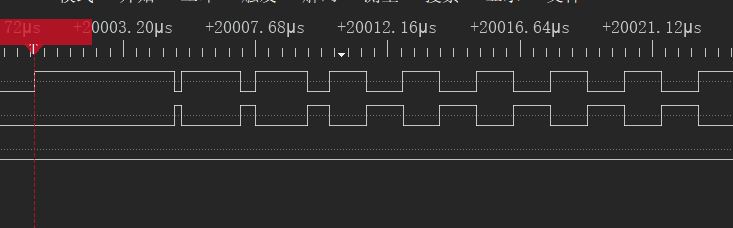
PWM Output Waveform
Code Overview
This section mainly introduces the code and process description for initialization and corresponding function implementation in the example.
Source Code Directory
The directory for project file and source code are as follows:
Project directory:
sdk\samples\peripheral\enhtimer\pwm+gdma\projSource code directory:
sdk\samples\peripheral\enhtimer\pwm+gdma\src
Initialization
The initialization flow for peripherals can refer to Initialization Flow in General Introduction.
-
Call
Pad_Config()andPinmux_Config()to configure the PAD and PINMUX of the corresponding pins.void board_enhance_pwm_init(void) { Pad_Config(PWM_OUT_P_PIN, PAD_PINMUX_MODE, PAD_IS_PWRON, PAD_PULL_NONE, PAD_OUT_DISABLE, PAD_OUT_LOW); Pad_Config(PWM_OUT_N_PIN, PAD_PINMUX_MODE, PAD_IS_PWRON, PAD_PULL_NONE, PAD_OUT_DISABLE, PAD_OUT_LOW); Pinmux_Config(PWM_OUT_P_PIN, PWM_PINMUX_OUT_P); Pinmux_Config(PWM_OUT_N_PIN, PWM_PINMUX_OUT_N); }
Call
RCC_PeriphClockCmd()to enable the GDMA clock.-
Initialize the GDMA peripheral:
Define the
GDMA_InitTypeDeftypeGDMA_InitStruct, and callGDMA_StructInit()to pre-fillGDMA_InitStructwith default values.Modify the
GDMA_InitStructparameters as needed. The initialization parameter configurations for GDMA are shown in the table below. CallGDMA_Init()to initialize the GDMA peripheral.
GDMA Hardware Parameters |
Setting in the |
GDMA |
|---|---|---|
Channel Num |
||
Source Data Size |
||
Destination Data Size |
||
Source Burst Transaction Length |
||
Destination Burst Transaction Length |
||
Destination Handshake |
||
Transfer Direction |
||
Source Address Increment or Decrement |
||
Destination Address Increment or Decrement |
||
Source Address |
|
|
Buffer Size |
4 |
|
Destination Address |
|
|
Secure function enable |
Call
RCC_PeriphClockCmd()to enable the ENHTIM clock.-
Initialize the ENHTIM peripheral:
Define the
ENHTIM_InitTypeDeftypeENHTIM_InitStruct, and callENHTIM_StructInit()to pre-fillENHTIM_InitStructwith default values.Modify the
ENHTIM_InitStructparameters as needed. The initialization parameter configurations for ENHTIM are shown in the table below. CallENHTIM_Init()to initialize the ENHTIM peripheral.
ENHTIM Hardware Parameters |
Setting in the |
ENHTIM |
|---|---|---|
Counter mode |
||
PWM mode |
||
Toggle output polarity |
||
Count value |
|
|
PWM deadzone clock source |
||
PWM deadzone function enable |
||
PWM P stop state |
||
PWM N stop state |
||
Size of deadzone time |
0x0 |
|
GDMA function enable |
||
GDMA target |
Call
GDMA_Cmd()to enable the GDMA peripheral and callENHTIM_Cmd()to enable the ENHTIM peripheral.
Functional Implementation
To better illustrate which parameters users can modify to achieve the desired waveform, the following example demonstrates how to obtain the waveform shown in the figure below:
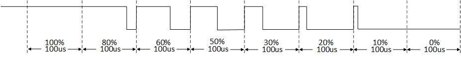
PWM with variable duty cycle
Determine the PWM Period: You can calculate it using the following formula: PWM_Period = Clock_Period * PWM_MAXCNT. Here, Clock_Period is 25 ns (based on a 40 MHz clock source). As illustrated, if a PWM waveform with a period of 100 us is desired, set the
PWM_MAXCNTmacro definition to 4000 in the Configuration Options.-
Determine the Duty Cycle: Organize the data to be entered into the CCR FIFO according to needs to set the duty cycle. For example, to generate a PWM waveform with a 100 µs period and duty cycles of 100%, 80%, 60%, 50%, 30%, 20%, 10%, and 0%, set the
GDMA_InitTypeDef::GDMA_BufferSizeto 8. Below is the ccr_fifo_buf data. For an 80% duty cycle, ccr_fifo_buf[1] should be set to 800. The calculation for the high-level duty cycle is: ((PWM_MAXCNT - CCR) / PWM_MAXCNT) = ((4000 - 800) / 4000) = 80%.static uint32_t ccr_fifo_buf[8] = {0, 800, 1600, 2000, 2800, 3200, 3600, 4000};
See Also
Please refer to the relevant API Reference: