3-Wire SPI
Sample List
This chapter introduces the details of the 3-Wire SPI sample code. The SDK provides the following samples for the 3-Wire SPI peripheral.
Functional Overview
3-Wire SPI is used to connect 3-Wire SPI interfaces such as CS/CLK/DATA and has single wire, single/burst read function. It is also possible to adjust the desired delay timing between read/write. The chip can write and read the sensor’s registers by 3-Wire SPI.
Note
Only RTL87x3D supports 3-Wire SPI.
Feature List
Support 2-wire and 3-wire communication.
Support single write.
Support single/burst read.
Configurable delay between write and read.
Half duplex.
Master only.
Block Diagram
Here is the overall IPs block diagram for 3-Wire SPI IP¹, which including ‘PAD/PINMUX’ for IO function configuration, ‘3-Wire SPI IP’ for 3-Wire SPI protocol.
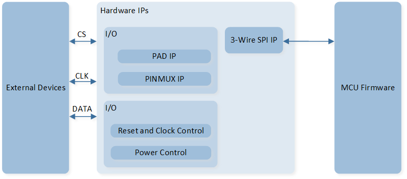
System Block Diagram of 3-Wire SPI
Transfer Protocol
Data Format
The data contains two bytes, the first byte is the address bit, the highest bit is the read/write control bit, and the second byte is the data byte. As shown below:
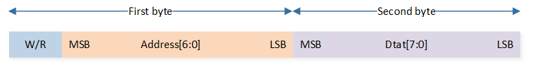
3-Wire SPI Data Format
Write Operation
Write data from the controller to the sensor, only supports single write mode, as shown in the figure below. No delay needs to be added between the address byte and the data byte.
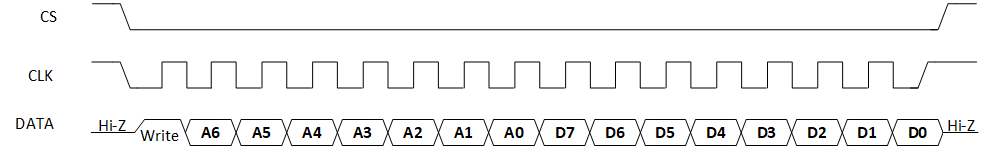
Schematic Diagram of 3-Wire SPI Write Operation Frame Format
Read Operation
Single Read Mode
Between the first byte (address byte) and the second byte (data byte), a delay of ‘T-Hold’ needs to be added. This delay is configured by SPI3WIRE_InitTypeDef::SPI3WIRE_ReadDelay.
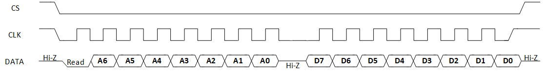
Schematic Diagram of 3-Wire SPI Single Read Operation Frame Format
Burst Read Mode
In burst read mode, SPI can continuously read multiple bytes of data. Between the first byte (address byte) and the second byte (data byte 0), a delay of ‘T-Hold’ needs to be added. This delay is configured by SPI3WIRE_InitTypeDef::SPI3WIRE_ReadDelay. There is no delay between the third byte (data byte 1) and the second byte (data byte 0) until the end of a burst read.
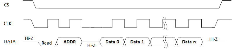
Schematic Diagram of 3-Wire SPI Burst Read Operation Frame Format
Power Manager
The 3-Wire SPI peripheral is located in the core domain and will be powered off in low power mode.
3-Wire SPI peripheral store/restore will be automatically performed based on whether the 3-Wire SPI clock is active.
Users can call the API io_dlps_register() to initialize 3-Wire SPI peripheral store/restore and do not need to worry about 3-Wire SPI peripheral requiring specific handling.