SDIO
Sample List
This chapter introduces the details of the SDIO sample. The SDK provides the following samples for the SDIO peripheral.
Functional Overview
SDIO card is an IO device that uses the SD bus and SD commands. SD card is a type of memory card that is used in newly emerging audio and video electronic devices. The shape and interface of the SDIO card are compatible with the SD card, but it not only realizes the storage function, but also realizes other functions, such as Bluetooth, Wireless Fidelity, etc. SD card has a total of 9 pins, including 2 ground pins, 1 power pin, 1 clock pin, 1 command pin, and 4 data pins. The host controls the internal operation of the SD card by reading or writing SD host controller.
Feature List
Support SD host standard specification V2.0.
Support 2 SD bus speed mode: default speed mode (frequency up to 25 MHz) and high speed mode (frequency up to 50 MHz).
Support 2 group pins on EVB to communicate with SD card. For specific pins, please refer to SDIO Group Pins in RTL87x3D or SDIO Group Pins in RTL87x3E and RTL87x3EP.
Support SD transmission mode of 1-bit mode (single-wire), 4-bit SD mode (four-wire).
Support optional bus clock, with a maximum of 50MHz for RTL87x3E and RTL87x3EP, and a maximum of 40MHz for RTL87x3D.
Support multiple block and single block transfer.
High voltage SD card: operation voltage 3.3V.
Support GDMA transfer.
Support interrupt control.
Block Diagram
Here is the overall IPs block diagram for SDIO IP, which including ‘PAD/PINMUX’ for IO function configuration, ‘SDIO IP’ for SDIO protocol and ‘DMAC IP’ for DMA access.
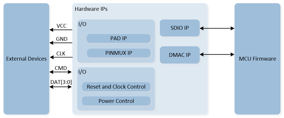
System Block Diagram of SDIO
Transfer Protocol
Communication over the SD bus is based on command and data bit streams that are initiated by a start bit and terminated by a stop bit. The control on the SD bus is realized through CMD, the host initiates a request, and then the SD card responds to the request. Data is transferred in the form of data blocks, and data blocks are always succeeded by CRC bits. For a multiple block write operation, the card will hold the DAT0 line low if its write buffer is full. Busy indication will be sent by the card to the host on DAT0 only.
Take the SD Bus multi-block read operation as an example:
The host sends a multi-block read command.
The SD card sends a response.
The card starts sending data.
After each block is sent, return a CRC status.
The card transmits the next block data.
Stop transmission until the host sends a stop command, the card responds.
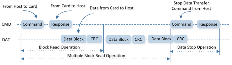
SD BUS Multiple Block Read Operation
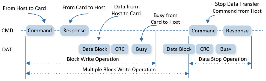
SD BUS Multiple Block Write Operation
Interface Definition
The connection of SD host controller (SDHC) and SD card is shown in SDHC and SD Card Connection Diagram.
Clock Line (CLK): host to card clock signal.
Command Line (CMD): bi-directional command and response signal.
Data Line (DAT0-DAT3): 4 bi-directional data signals.
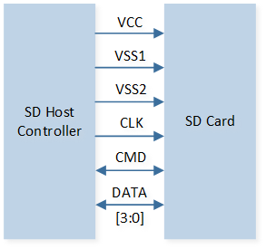
SDHC and SD Card Connection Diagram
The SDIO group pins of different ICs are shown in the tables below. RTL87x3EP is the same as RTL87x3E.
RTL87x3D |
CLK |
CMD |
DAT0 |
DAT1 |
DAT2 |
DAT3 |
|---|---|---|---|---|---|---|
Group0 Pins |
P1_2 |
P1_3 |
P1_4 |
P1_5 |
P1_6 |
P1_7 |
Group1 Pins |
P4_2 |
P4_3 |
P4_4 |
P4_5 |
P4_6 |
P4_7 |
RTL87x3E/EP |
CLK |
CMD |
DAT0 |
DAT1 |
DAT2 |
DAT3 |
|---|---|---|---|---|---|---|
Group0 Pins |
P5_0 |
P5_1 |
P5_2 |
P5_3 |
P5_4 |
P5_5 |
Group1 Pins |
P6_0 |
P6_1 |
P6_2 |
P6_3 |
P6_4 |
P6_5 |
Power Manager
The SDIO peripheral is located in the core domain and will be powered off in low power mode.
SDIO peripheral store/restore will be automatically performed based on whether the SDIO clock is active.
Users can call the API io_dlps_register() to initialize SDIO peripheral store/restore and do not need to worry about SDIO peripheral requiring specific handling.
Troubleshooting
How to Debug SD Initialization Failure Issue?
If the SD card has a CMD8 response error during the card identification stage, it is usually caused by external environmental factors.
Check whether the power supply voltage of the pin group is 3.3V: verify the power supply of the corresponding IO domain and LDO.
Check whether the SDIO pins of the package used are supported.
Check whether the card connection is stable.
Check whether the card responds after the host sends CMD.