SPI
Sample List
This chapter introduces the details of the SPI sample. The SDK provides the following samples for the SPI peripheral.
Functional Overview
The serial peripheral interface (SPI) allows half/full-duplex, synchronous, serial communication with external devices. The interface can be configured in one of two modes of operations: as a serial master or a serial slave. In master mode, it provides the communication clock (SCK) to the external slave device. SPI0 can be the master or slave, SPI1 and SPI2 is the master.
Feature List
Support master and slave modes.
Support 4 clock modes (CPOL=0/1, CPHA=0/1).
SCK frequency = SPIx_CLK/N, N is any even value between 2 and 65534.
Support 4 to 32 bits data frame in master mode.
Support 4 to 16 bits data frame in slave mode in RTL87x3D, 4/8/16 bits data frame in slave mode in RTL87x3E and RTL87x3EP.
Support up to 3 slave devices in master mode.
Support GDMA.
The maximum SPI clock supported by SPI in master mode and slave mode is as follows.
IC Type |
SPI0 Master Max Clock (MHz) |
SPI1 Master Max Clock (MHz) |
SPI2 Master Max Clock (MHz) |
SPI0 Slave Max Clock (MHz) |
|---|---|---|---|---|
|
50 (with dedicated I/Os) 10 (with general I/Os) |
20 (with dedicated I/Os) 10 (with general I/Os) |
20 (with dedicated I/Os) 10 (with general I/Os) |
10 |
|
|
50 (with dedicated I/Os) 10 (with general I/Os) |
20 (with dedicated I/Os) 10 (with general I/Os) |
20 (with dedicated I/Os) 10 (with general I/Os) |
10 |
|
|
40 (with dedicated I/Os) 10 (with general I/Os) |
20 (with dedicated I/Os) 10 (with general I/Os) |
20 (with dedicated I/Os) 10 (with general I/Os) |
10 |
Note
RTL87x3D, RTL87x3E, and RTL87x3EP support 3 SPI. SPI0 supports master mode and slave mode. SPI1 and SPI2 only support master mode.
SPI0 and SPI1 support 3 slave devices in master mode, and SPI2 supports 1 slave device in master mode.
If the user needs to operate flash and read data from flash, it is recommended to use
SPI_Direction_EEPROMmode. In this mode, the SPI controller will automatically supplement the padding bits needed for reading back. Set the read data length bySPI_SetReadLen()before reading from flash, then the result ofSPI_GetRxFIFOLen()will equal this value. IfSPI_Direction_FullDuplexmode is used when operating flash, it needs to supplement the padding bits manually, and the number of bytes should be equal to the read data length. In this way, the result ofSPI_GetRxFIFOLen()is the total length of padding bits and data to read.SPI_SetReadLen()is just forSPI_Direction_EEPROMmode.SPI support up to 50MHz (SPI0 of RTL87x3E and RTL87x3EP), 40MHz (SPI0 of RTL87x3D) and 20MHz (SPI1 and SPI2) with dedicated I/Os, support 10MHz with general I/Os. For dedicated I/O, please refer to the HDK related documentation.
Block Diagram
Here is the overall IPs block diagram for SPI IP, which including ‘PAD/PINMUX’ for IO function configuration, ‘SPI IP’ for SPI protocol and ‘DMAC IP’ for DMA access.
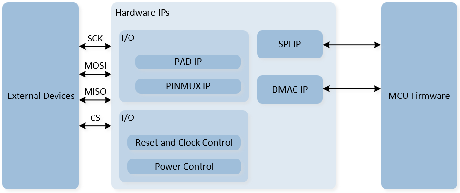
System Block Diagram of SPI
Communication Sequence Diagram
SPI supports 4 clock modes, corresponding to the four cases where CPOL and CPHA are 0 and 1. Please refer to the table SPI Clock Mode.
Clock Polarity (CPOL) bit sets the polarity of the clock signal in idle state. 0 indicates low level, and 1 indicates high level.
Clock Phase (CPHA) bit sets the edge on which data is captured: 0 indicates the first edge, and 1 indicates the second edge.
SPI Mode |
Clock Polarity (CPOL) |
Clock Phase (CPHA) |
|---|---|---|
Mode 0 |
0 |
0 |
Mode 1 |
0 |
1 |
Mode 2 |
1 |
0 |
Mode 3 |
1 |
1 |
The diagrams below illustrate the SPI communication timing for each of the four modes.
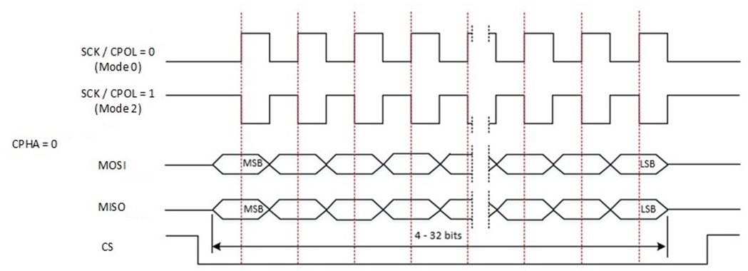
SPI Communication Sequence Diagram (SCPH is 0)
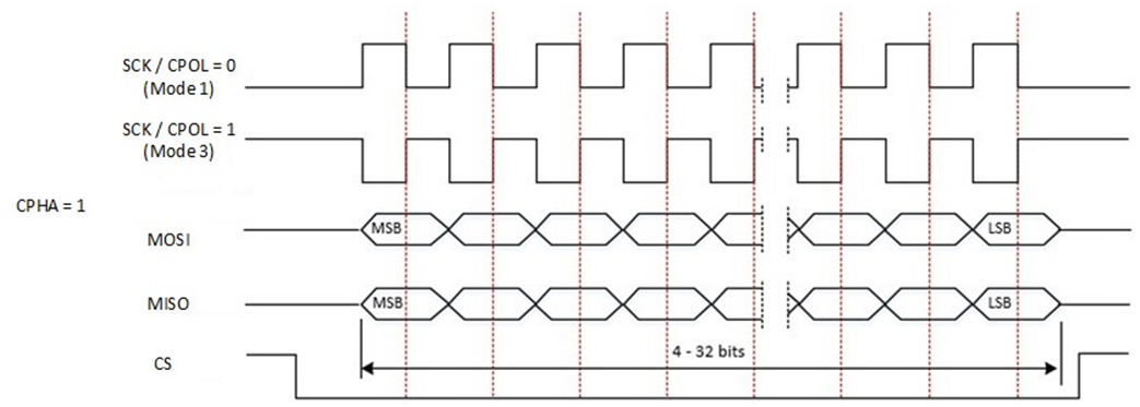
SPI Communication Sequence Diagram (SCPH is 1)
Transfer Mode
SPI supports four transmission modes:
-
Full Duplex Mode
In full duplex mode, both the data transmission and reception logic are active. Therefore, attention must be paid to the logic of data transmission and reception during communication. Configure
SPI_InitTypeDef::SPI_DirectiontoSPI_Direction_FullDuplex. -
Transmit Only Mode
In transmit only mode, only the transmission logic is active, and the reception logic is inactive; received data will not be stored in the RX FIFO. Configure
SPI_InitTypeDef::SPI_DirectiontoSPI_Direction_TxOnly. -
Receive Only Mode
In receive only mode, only the reception logic is active, and the transmission logic is inactive. Configure
SPI_InitTypeDef::SPI_DirectiontoSPI_Direction_RxOnly. -
EEPROM Mode
EEPROM mode is typically used to send opcodes or addresses to EEPROM devices. In EEPROM mode, SPI first sends data until the TX FIFO is empty, then begins receiving data. During data transmission, the reception logic is inactive. During data reception, the transmission logic is inactive. Configure
SPI_InitTypeDef::SPI_DirectiontoSPI_Direction_EEPROM. In EEPROM mode, theSPI_InitTypeDef::SPI_NDFvalue must be set to determine the quantity of data to be received.
High Speed
This section provides an overview of the high-speed for SPI interfaces, detailing configurations for both SPI Master and SPI slave to achieve faster data transmission.
Master High Speed
SPI0 supports high-speed mode. When the SPI transmission rate exceeds 20MHz, it is recommended to use the high-speed mode of SPI0, and it is also recommended to use it with GDMA. In high-speed mode, the peripheral base address should be selected as SPI0_HS, and dedicated pins should be used. For details, please refer to the demo code in sdk\src\sample\io_demo\spi\spi0_hs\spi0_hs_dma_demo.c.
Slave High Speed
The SPI slave needs to adjust the slow clock to support high speed, as shown in SPI Slow Clock Settings in RTL87x3E and SPI Slow Clock Settings in RTL87x3D.
For details, please refer to the demo code in src\sample\io_demo\spi\slave\spi_slave_tx_dma_hs_demo.c and src\sample\io_demo\spi\slave\spi_slave_rx_dma_hs_demo.c.
SPI Clock Div |
SPI Clock |
Slave RX Slow Clock |
Slave TX Slow Clock |
|---|---|---|---|
16 |
2.5MHz |
/ |
1.25MHz |
10 |
4MHz |
/ |
1.25MHz |
8 |
5MHz |
/ |
2.5MHz |
4 |
10MHz |
2.5M |
4MHz |
SPI Clock Div |
SPI Clock |
Slave TX Slow Clock |
|---|---|---|
8 |
5MHz |
2.5MHz |
4 |
10MHz |
5MHz |
External Flash
This section introduces how to communicate with external flash by SPI. Please refer to SPI External Flash for demo code and refer to SPI Sample Code Hardware Connection Diagram for hardware connection.
Hardware Connection
Users need to modify the pins related to external flash in the code according to the hardware design. The macro definition below shows the pins defined in the code.
#define FLASH_SCK                   P5_0
#define FLASH_MOSI                  P5_2
#define FLASH_MISO                  P5_3
#define FLASH_CS                    P5_1
#define FLASH_HOLD                  P5_5
Demo Code
Users can implement functions to communicate with external flash by referring to the demo code in SPI External Flash.
Commands for External Flash
Different flash models may have different commands, and users can modify the following definitions according to the flash specifications.
typedef enum
{
   EXT_FLASH_WRITE_STATUS_CMD      = 0x01,
   EXT_FLASH_PROGRAM_CMD           = 0x02,
   EXT_FLASH_READ_CMD              = 0x03,
   EXT_FLASH_WRITE_DISABLE_CMD     = 0x04,
   EXT_FLASH_READ_STATUS_CMD       = 0x05,
   EXT_FLASH_WRITE_ENABLE_CMD      = 0x06,
   EXT_FLASH_SECTOR_ERASE_CMD      = 0x20,
   EXT_FLASH_BLOCK_ERASE_32_CMD    = 0x52,
   EXT_FLASH_CHIP_ERASE_CMD        = 0x60,
   EXT_FLASH_BLOCK_ERASE_64_CMD    = 0xd8,
   EXT_FLASH_READ_ID_CMD           = 0x9F,
   EXT_FLASH_RELEASE_DEEP_SLEEP    = 0xAB,
   EXT_FLASH_DEEP_SLEEP            = 0xB9,
   EXT_FLASH_SOFTWARE_RESET_ENABLE = 0x66,
   EXT_FLASH_SOFTWARE_RESET        = 0x99,
} EXT_FLASH_OPERATION_CMD;
Initialization of External Flash
Users can refer to the following function to initialize external flash. In this function, it will initialize SPI and reset external flash.
void ext_flash_spi_init(void)
Erase External Flash
Users can refer to the following function to erase external flash. Sector, block, and chip are the three common erase commands used for flash.
EXT_FLASH_SPI_OPERATION_STATUS ext_flash_spi_erase(uint32_t address, EXT_FLASH_OPERATION_CMD mode)
Write External Flash
Users can refer to the following function to write external flash by polling mode.
EXT_FLASH_SPI_OPERATION_STATUS ext_flash_spi_page_program(uint32_t address, uint8_t *psendBuf, uint16_t len)
Users can refer to the following function to write external flash by interrupt mode.
EXT_FLASH_SPI_OPERATION_STATUS ext_flash_spi_page_program_by_interrupt(uint32_t address, uint8_t *psendBuf, uint16_t len)
Users can refer to the following function to write external flash by GDMA mode.
EXT_FLASH_SPI_OPERATION_STATUS ext_flash_spi_page_program_by_dma(uint32_t address, uint8_t *psendBuf, uint16_t len)
Read External Flash
Users can refer to the following function to read external flash by polling mode.
EXT_FLASH_SPI_OPERATION_STATUS ext_flash_spi_read(uint32_t address, uint8_t *pStoreBuf, uint16_t len)
Users can refer to the following function to read external flash by interrupt mode.
EXT_FLASH_SPI_OPERATION_STATUS ext_flash_spi_read_by_interrupt(uint32_t address, uint8_t *pStoreBuf, uint16_t len)
Users can refer to the following function to read external flash by GDMA mode.
EXT_FLASH_SPI_OPERATION_STATUS ext_flash_spi_read_by_dma(uint32_t address, uint8_t *pStoreBuf, uint16_t len)
Slave Note
The SPI slave does not support TX FIFO underflow conditions. The TX FIFO needs to be filled with data before the SPI master starts the transfer. There are two methods to avoid this condition:
Send data to the SPI slave TX FIFO before transmission, then toggle a GPIO to notify the SPI master to send data. For the specific implementation, please refer to the demo code in
src\sample\io_demo\spi\slave\spi_slave_gpio_demo.c.Use GDMA for the SPI slave to send data: Enable TX GDMA immediately after SPI slave init to ensure that there is always data in the SPI slave TX FIFO.
Note
If TX FIFO underflow occurs, users can reset SPI slave to recover.
For details, please refer to src\sample\io_demo\spi\slave\spi_slave_tx_dma_hs_demo.c.
GDMA Flow Based on GPIO Indication
This section introduces SPI slave transfers based on GPIO Indication when communicating with the SPI master in GDMA mode. The SPI slave must send data to the TX FIFO before the SPI master starts to communicate with the SPI slave; Otherwise, it will trigger TX FIFO underflow error interrupt for the SPI slave. Users can use GPIO to control the timing between the SPI master and the SPI slave. A GPIO pin needs to be toggled for the SPI slave to indicate that the TX data is ready, and the SPI master can transfer data afterward. For the detailed flow, please refer to SPI MISO Flow Chart.
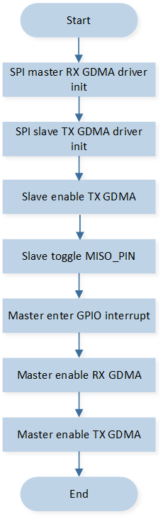
SPI MISO Flow Chart
GDMA Note
If SPI is operated in CPU mode with GDMA handshake enabled, it may cause GDMA to get the false signal. So if it’s needed for SPI to read or write by GDMA after CPU mode, the GDMA handshake must be reset before starting GDMA.
SPI_GDMACmd(FLASH_SPI, SPI_GDMAReq_Rx, DISABLE);
SPI_GDMACmd(FLASH_SPI, SPI_GDMAReq_Rx, ENABLE);
GDMA_Cmd(SPI_RX_DMA_CHANNEL_NUM, ENABLE);
Power Manager
The SPI peripheral is located in the core domain and will be powered off in low power mode.
SPI peripheral store/restore will be automatically performed based on whether the SPI clock is active.
Users can call the API io_dlps_register() to initialize SPI peripheral store/restore and do not need to worry about SPI peripheral requiring specific handling.
For more details, please refer to the demo code in SPI Master DLPS and SPI Slave DLPS.
Troubleshooting
How to Debug SPI Data Transfer Failures?
Check if any error interrupt status is triggered.
When using the slave TX function, check if the slave sends data to the TX FIFO before the SPI master starts the transfer.
If using DMA mode, check if DMA is reinitialized after exiting dlps.