SPI Write Polling Receive Interrupt
This document introduces three SPI communication samples. The sample1 demonstrates how SPI1 master sends and receives data using polling mode. The sample2 demonstrates how SPI1 master sends data using polling and receives data by interrupt mode. The sample3 demonstrates how SPI0 slave receives data using interrupt mode. In all three examples, SPI direction is full-duplex, and the clock is set to 400KHz. The chip writes data to the SPI slave and reads data from it.
Requirements
For hardware requirements, please refer to the Requirements.
Wiring
Sample 1 Wiring
Connect P1_2 (master SCK) to SCK of SPI slave device, connect P1_3 (master MOSI) to MOSI of SPI slave device, connect P1_4 (master MISO) to MISO of SPI slave device, and connect P1_5 (master CS) to CS of SPI slave device. The hardware connection of SPI sample code is shown in the figure below.
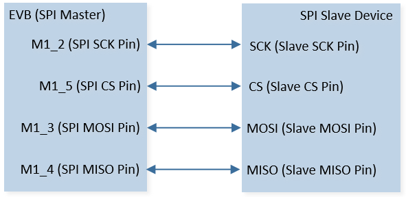
SPI Sample Code Hardware Connection Diagram
Sample 2 Wiring
Connect P0_0 (master SCK) to SCK of SPI slave device, connect P1_0 (master MOSI) to MOSI of SPI slave device, connect P1_1 (master MISO) to MISO of SPI slave device, and connect P0_1 (master CS) to CS of SPI slave device. The hardware connection of SPI sample code is shown in the figure below.
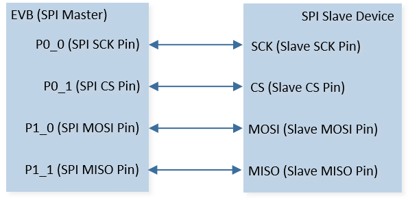
SPI Sample Code Hardware Connection Diagram
Sample 3 Wiring
Connect MIC1_P (slave SCK) to SCK of SPI master device, connect MIC2_P (slave MOSI) to MOSI of SPI master device, connect MIC1_N (slave MISO) to MISO of SPI master device, and connect MIC2_N (slave CS) to CS of SPI master device. The hardware connection of SPI sample code is shown in the figure below.
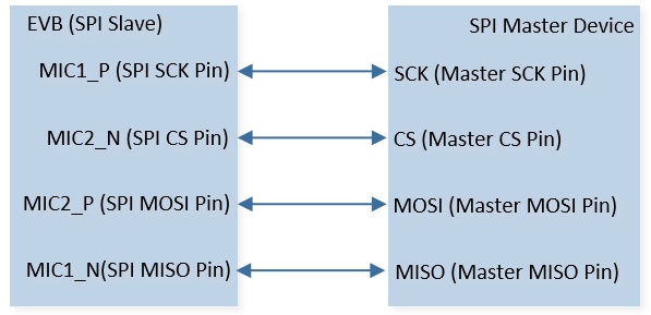
SPI Sample Code Hardware Connection Diagram
Configurations
-
The following macros can be configured to modify pin definitions for sample1.
#define PIN_SPI1_SCK P1_2#define PIN_SPI1_MOSI P1_3#define PIN_SPI1_MISO P1_4#define PIN_SPI1_CS P1_5
-
The following macros can be configured to modify pin definitions for sample2.
#define PIN_SPI1_SCK P0_0#define PIN_SPI1_MOSI P1_0#define PIN_SPI1_MISO P1_1#define PIN_SPI1_CS P0_1
-
The following macros can be configured to modify pin definitions for sample3.
#define PIN_SPI0_SCK MIC1_P#define PIN_SPI0_MOSI MIC2_P#define PIN_SPI0_MISO MIC1_N#define PIN_SPI0_CS MIC2_N
-
The entry function are as follows, call this function in
main()to run this sample code. For more details, please refer to the Initialization.For sample 1, use the following entry function:
spi_demo();
For sample 2, use the following entry function:
spi_master_demo();
For sample 3, use the following entry function:
spi_slave_demo();
Building and Downloading
For building and downloading, please refer to the Building and Downloading.
Experimental Verification
Sample 1 Verification
Press the Reset button on the EVB, the data in the array
SPI_WriteBufis sent to SPI slave device.-
If the slave device sends the same data to the chip, the chip stores the received data in array
SPI_ReadBufand prints the data in Debug Analyzer.spi_demo: SPI_ReadBuf[0] 0x9f spi_demo: SPI_ReadBuf[1] 0x1 spi_demo: SPI_ReadBuf[2] 0x2 spi_demo: SPI_ReadBuf[3] 0x0
Sample 2 Verification
Press the Reset button on the EVB, the data in the array
SPI_WriteBufis sent to SPI slave device.-
After the slave device sends data to the chip, when the data length in RX FIFO is equal to or above its threshold value plus 1, trigger the
SPI_INT_RXFinterrupt. Then the data is received in arraySPI_ReadINTBufand printed in Debug Analyzer.spi1_handler: SPI_ReadINTBuf[0] 0x%x ... spi1_handler: SPI_ReadINTBuf[len] 0x%x
Sample 3 Verification
Press the Reset button on the EVB.
-
After the slave device sends data to the chip, when the data length in RX FIFO is equal to or above its threshold value plus 1, trigger the
SPI_INT_RXFinterrupt. Then the data is received in arraySPI_ReadINTBufand printed in Debug Analyzer.spi0_handler: SPI_ReadINTBuf[0] 0x%x ... spi0_handler: SPI_ReadINTBuf[len] 0x%x
Code Overview
Source Code Directory
For both samples, please refer to the Source Code Directory for the project directory.
Sample 1 source code:
Source code directory:
sdk\src\sample\io_demo\spi\polling\spi_demo.c.
Sample 2 source code:
Source code directory:
sdk\src\sample\io_demo\spi\interrupt\spi_master_demo.c.
Sample 3 source code:
Source code directory:
sdk\src\sample\io_demo\spi\slave\spi_slave_demo.c.
TX Polling Initialization Flow
The initialization flow for peripherals can refer to Initialization Flow.
SPI TX polling initialization flow is shown in the following figure.
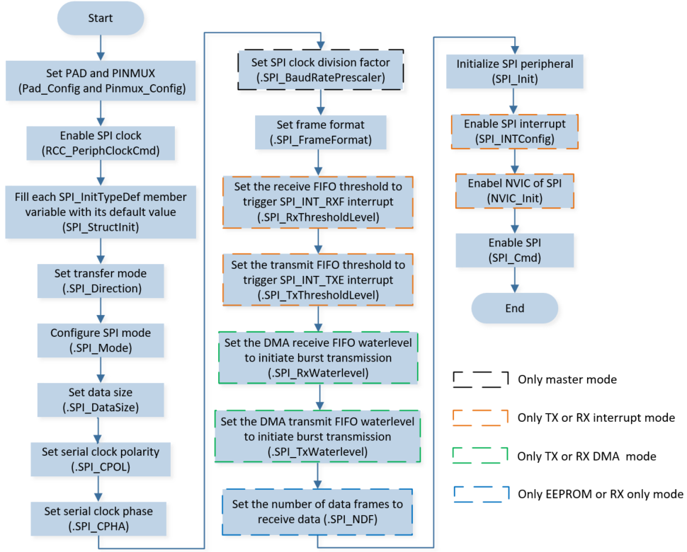
SPI Initialization Flow Chart
-
Call
Pad_Config()andPinmux_Config()to initialize the pins.static void board_spi_init(void) { Pinmux_Config(PIN_SPI1_SCK, SPI1_CLK_MASTER); Pinmux_Config(PIN_SPI1_MOSI, SPI1_MO_MASTER); Pinmux_Config(PIN_SPI1_MISO, SPI1_MI_MASTER); Pinmux_Config(PIN_SPI1_CS, SPI1_SS_N_0_MASTER); Pad_Config(PIN_SPI1_SCK, PAD_PINMUX_MODE, PAD_IS_PWRON, PAD_PULL_NONE, PAD_OUT_ENABLE, PAD_OUT_HIGH); Pad_Config(PIN_SPI1_MOSI, PAD_PINMUX_MODE, PAD_IS_PWRON, PAD_PULL_NONE, PAD_OUT_ENABLE, PAD_OUT_HIGH); Pad_Config(PIN_SPI1_MISO, PAD_PINMUX_MODE, PAD_IS_PWRON, PAD_PULL_NONE, PAD_OUT_ENABLE, PAD_OUT_HIGH); Pad_Config(PIN_SPI1_CS, PAD_PINMUX_MODE, PAD_IS_PWRON, PAD_PULL_NONE, PAD_OUT_ENABLE, PAD_OUT_HIGH); }
Call
RCC_PeriphClockCmd()to enable the SPI clock and function.-
Initialize the SPI peripheral:
Define the
SPI_InitTypeDeftypeSPI_InitStructure, and callSPI_StructInit()to pre-fillSPI_InitStructurewith default values.Modify the
SPI_InitStructureparameters as needed. The SPI initialization parameter configuration is shown in the table below.Call
SPI_Init()to initialize the SPI peripheral.
SPI Initialization Parameters SPI Hardware Parameters
Setting in the
SPI_InitStructureSPI
Direction
Device Role (SPI Master or SPI Slave)
Data Frame Size
Clock Polarity
Clock Phase
Clock Div
100
Frame Format
Call
SPI_Cmd()to enable SPI.
RX Interrupt Initialization Flow
The initialization flow for peripherals can refer to Initialization Flow.
SPI RX interrupt initialization flow can refer to SPI Initialization Flow Chart.
Both sample 2 and 3 have the RX interrupt function and the initialization flow is the same. The difference is that sample 2 uses SPI1 as the master and sample 3 uses SPI0 as the slave. The following is a detailed description using sample 2 as an example.
-
Call
Pad_Config()andPinmux_Config()to initialize the pins.static void board_spi_init(void) { Pinmux_Config(PIN_SPI1_SCK, SPI1_CLK_MASTER); Pinmux_Config(PIN_SPI1_MOSI, SPI1_MO_MASTER); Pinmux_Config(PIN_SPI1_MISO, SPI1_MI_MASTER); Pinmux_Config(PIN_SPI1_CS, SPI1_SS_N_0_MASTER); Pad_Config(PIN_SPI1_SCK, PAD_PINMUX_MODE, PAD_IS_PWRON, PAD_PULL_NONE, PAD_OUT_ENABLE, PAD_OUT_HIGH); Pad_Config(PIN_SPI1_MOSI, PAD_PINMUX_MODE, PAD_IS_PWRON, PAD_PULL_NONE, PAD_OUT_ENABLE, PAD_OUT_HIGH); Pad_Config(PIN_SPI1_MISO, PAD_PINMUX_MODE, PAD_IS_PWRON, PAD_PULL_NONE, PAD_OUT_ENABLE, PAD_OUT_HIGH); Pad_Config(PIN_SPI1_CS, PAD_PINMUX_MODE, PAD_IS_PWRON, PAD_PULL_NONE, PAD_OUT_ENABLE, PAD_OUT_HIGH); }
Call
RCC_PeriphClockCmd()to enable the SPI clock and function.-
Initialize the SPI peripheral:
Define the
SPI_InitTypeDeftypeSPI_InitStructure, and callSPI_StructInit()to pre-fillSPI_InitStructurewith default values.Modify the
SPI_InitStructureparameters as needed. The SPI initialization parameter configuration is shown in the table below.Call
SPI_Init()to initialize the SPI peripheral.
SPI Initialization Parameters SPI Hardware Parameters
Setting in the
SPI_InitStructureSPI
Direction
Device Role (SPI Master or SPI Slave)
Data Frame Size
Clock Polarity
Clock Phase
Clock Div
100
Frame Format
Receive FIFO Threshold Level
0
Call
RamVectorTableUpdate()to register SPI interrupt handler.Call
SPI_INTConfig()to enable RX FIFO full interruptSPI_INT_RXF.Call
NVIC_Init()to enable NVIC of SPI.Call
SPI_Cmd()to enable SPI.
Functional Implementation
Send Data by Polling
Call
SPI_SendBuffer()to send the data inSPI_WriteBufto the slave.Call
SPI_GetFlagState()to checkSPI_FLAG_BUSYflag state, and wait for the SPI data transfer to complete.
uint8_t SPI_WriteBuf[16] = {0, 0x01, 0x02, 0x00};

SPI_WriteBuf[0] = 0x9f;
SPI_SendBuffer(SPI1, SPI_WriteBuf, 4);

while (SPI_GetFlagState(SPI1, SPI_FLAG_BUSY));
Receive Data by Interrupt
-
When the receive buffer reaches or goes above the RX FIFO threshold level (
SPI_InitTypeDef::SPI_RxThresholdLevel+ 1), RX full interrupt will be triggered and enters the interrupt handler:Call
SPI_GetINTStatus()to checkSPI_INT_RXFinterrupt status.Call
SPI_GetRxFIFOLen()to get the data length in RX FIFO.Call
SPI_ReceiveData()to receive data from RX FIFO.
static void spi1_handler(void)
{
   uint8_t len = 0;
   uint8_t idx = 0;
   uint8_t SPI_ReadINTBuf[16] = {0, 0, 0, 0};

   if (SPI_GetINTStatus(SPI1, SPI_INT_RXF) == SET)
   {
      /* It is recommended to post the os msg to the task thread for data processing. */
      len = SPI_GetRxFIFOLen(SPI1);
      for (idx = 0; idx < len; idx++)
      {
            /* must read all data in receive FIFO , otherwise cause SPI_INT_RXF interrupt again */
            SPI_ReadINTBuf[idx] = SPI_ReceiveData(SPI1);
            IO_PRINT_INFO2("spi1_handler: SPI_ReadINTBuf[%d] 0x%x", idx, SPI_ReadINTBuf[idx]);
      }
   }
}