I2S
Sample List
This chapter introduces the details of the I2S sample code. List the sample code supported for different IC s.
Functional Overview
I2S interface can support audio protocols such as I2S, Left-Justified, PCM, and TDM. Through the I2S interface, RTL87x3E and RTL87x3D can bridge to an external DSP core (or audio codec/audio amplifier). I2S can be operated in GDMA mode or FIFO mode. Set the buffer size according to the amount of transferred data in GDMA mode, or access I2S FIFO directly to transmit and receive data in FIFO mode. It is recommended to transfer the audio data via GDMA automatically since it can reduce the number of interrupts and improve efficiency.
Feature List
Support 16/20/24/32 bits data resolution (data width).
Support 16/20/24/32 bits word length (channel width).
Support non-TDM (2-ch), TDM4 (4-ch), TDM6 (6-ch), and TDM8 (8-ch).
Support master and slave mode.
Support GDMA handshake operation.
Block Diagram
Here is the overall IPs block diagram for I2S IP, which including ‘PAD/PINMUX’ for IO function configuration, ‘I2S IP’ for I2S protocol, ‘DMAC IP’ for GDMA access.
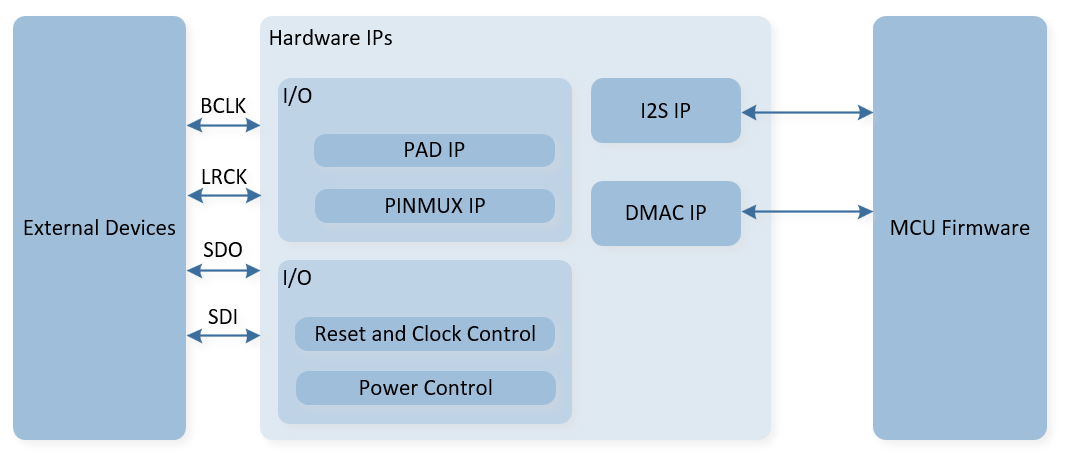
System Block Diagram of I2S
Clock Divider
-
BCLK fractional divider according to the following equation: BCLK = XTAL 40MHz * (
I2S_InitTypeDef::I2S_BClockNi/I2S_InitTypeDef::I2S_BClockMi).Example: For XTAL 40MHz clock source to generate 12.288MHz BCLK case. It’s recommended to use the settings of
I2S_InitTypeDef::I2S_BClockNi= 192 andI2S_InitTypeDef::I2S_BClockMi= 625.Note that because the clock source comes from XTAL 40MHz, BCLK would be a jittered clock composed of 10MHz and 13.33MHz in practice.
-
Set even-bit integer divider for LRCK according to the following equation: LRCK = BCLK / (
I2S_InitTypeDef::I2S_BClockDiv+ 1).Where
I2S_InitTypeDef::I2S_BClockDivcould be calculated by:I2S_InitTypeDef::I2S_BClockDiv= (channel width * channel number) - 1.The channel number is determined by the TDM (Time Division Multiplexing) mode, 2-channels for without-TDM mode, 4-channels for TDM4 mode, and so on.
The recommended clock divider setting for 2-channels & 32-bit channel width is shown below.
BCLK Frequency |
Clock Source |
Sampling Rate |
|||
0.512 MHz |
XTAL 40MHz |
8 |
625 |
63 |
8 KHz |
0.768 MHz |
XTAL 40MHz |
12 |
625 |
63 |
12 KHz |
1.024 MHz |
XTAL 40MHz |
16 |
625 |
63 |
16 KHz |
1.536 MHz |
XTAL 40MHz |
24 |
625 |
63 |
24 KHz |
2.048 MHz |
XTAL 40MHz |
32 |
625 |
63 |
32 KHz |
3.072 MHz |
XTAL 40MHz |
48 |
625 |
63 |
48 KHz |
6.144 MHz |
XTAL 40MHz |
96 |
625 |
63 |
96 KHz |
12.288 MHz |
XTAL 40MHz |
192 |
625 |
63 |
192 KHz |
2.8224 MHz |
XTAL 40MHz |
441 |
6250 |
63 |
44.1 KHz |
5.6448 MHz |
XTAL 40MHz |
441 |
3125 |
63 |
88.2 KHz |
0.7056 MHz |
XTAL 40MHz |
441 |
25000 |
63 |
11.025 KHz |
1.4112 MHz |
XTAL 40MHz |
441 |
12500 |
63 |
22.05 KHz |
As mentioned above, I2S BCLK is a jittered clock composed of two frequencies that are generated from XTAL 40MHz. The clock jitter percentage generated from XTAL 40MHz is shown in below.
BCLK (MHz) |
Clock Jitter Percentage (%) |
|
Sampling Rate 48KHz Group |
1.024 |
1.132 |
2.048 |
1.032 |
|
3.072 |
1.772 |
|
6.144 |
1.297 |
|
12.288 |
1.627 |
|
Sampling Rate 44.1KHz Group |
2.8224 |
1.241 |
5.6448 |
1.261 |
|
11.2896 |
1.24 |
LRCK (KHz) |
Clock Jitter Percentage (%) |
16 |
0 |
48 |
0.08 |
96 |
0.179 |
44.1 |
0.107 |
88.2 |
0.114 |
192 |
0.168 |