CFU
CFU uses Microsoft's open-source license, and the corresponding website is https://learn.microsoft.com/en-us/windows-hardware/drivers/cfu/. CFU provides OEMs and Independent Hardware Vendors (IHVs) with a reliable and authenticated method for updating firmware on devices that have shipped to customers. The SDK supports the CFU protocol defined by Microsoft. As shown in Flash, there are two bank areas allocated (bank0 and bank1) to save the images, but only one bank is active at a time. The images in the two banks will be authenticated when the SoC boots up. If the images in both banks are all valid, the bank with the higher version will be selected to run. The versions of the images in the two banks will be compared in a specific sequence until a difference is found. If only one bank's images are all valid, then this bank will be selected to run. Detailed instructions on bank switching can be found in OTA. For CFU, all the images in both banks should be packed together, and the CFU tool will automatically select the images to transfer to the inactive bank.
This user manual describes CFU-related information. The following topics are included to help users establish a CFU environment.
CFU Flow
HID Interface
CFU Protocol
Code Overview
Experimental Verification
CFU Flow
Images pushed by the CFU tool will always be saved in the inactive bank during the CFU process. The MCU will reboot after all images have been pushed and validated successfully. The advantage of dual bank CFU is that there is always a backup bank, so users do not need to worry about the SoC crashing if the CFU process fails. Because the bank with all valid images and higher versions will be selected to be activated by the bootloader, the upgraded images should have higher versions and be integrated. Otherwise, the images will not be activated when the chip reboots.
Dual Bank CFU Mode
The dual bank CFU flow is shown in the following chart.
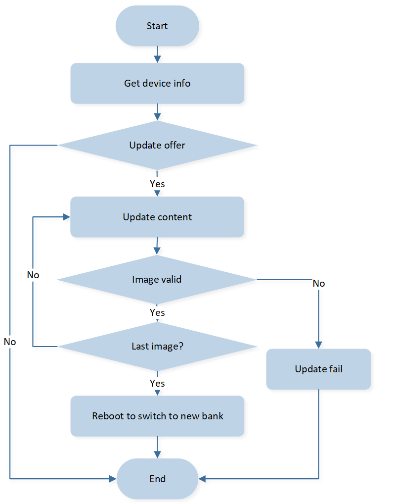
Flow of Dual Bank CFU
HID Interface
Devices supporting CFU implement a set of reports contained in a vendor-specific Top-Level Collection. A Top-Level Collection comprises a set of reports. This set of HID reports is abstracted into a set of Collections and Main Items (controls) with their corresponding attributes such as Usage, valid value ranges, and sizes. Windows enumerates each TLC separately in its own Physical Device Object (PDO) that drivers can attach to. Software then addresses Collections and Main Items, and the HID stack takes care of translating those into reports sent to and received from the HID Class device.
A HID Interface may have one or more peer TLCs. The TLCs of a HID Interface are described by a read-only structure delivered during enumeration called a Report Descriptor, in which the attributes of the sub-collections and their Main Items are described and assigned to reports.
HID Utility Top-Level Collection
Devices supporting CFU implement a set of fixed-size reports contained in a vendor-specific Top-Level Collection called the Utility TLC. The Utility TLC defines several reports, not all of which are always implemented in a device. Unused reports are intended for future expansion. All reports defined in the Utility TLC are always defined even if they are not implemented. This permits future firmware updates to enable new reports without changing the HID Report Descriptor. Changing the Report Descriptor for an enumerated HID device after an update causes interoperability issues due to operating systems that cache information in the Report Descriptor between enumerations. Every report on a HID interface that contains more than 1 report must have a Report ID, and the Report ID is defined to be the first byte of all reports on the interface.
SFUA TLC |
Usage |
Report ID |
Desc |
Usage |
Report ID |
Desc |
Usage |
Report ID |
Desc |
|---|---|---|---|---|---|---|---|---|---|
Page ID |
0x60 |
0x2A |
FW Version Response |
0x61 |
0x62 |
0x2A |
FW Version Request |
||
0xFF0B: 0x0104 |
0x63 |
0x64 |
0x65 |
0x2B |
FW Version Request Ex |
||||
0x66- 0x69 |
0x2C |
FW Update Response |
0x6A- 0x6D |
0x6E- 0x71 |
|||||
0x72- 0x75 |
0x76- 0x79 |
0x7A- 0x7D |
|||||||
0x7E- 0x81 |
0x82- 0x85 |
0x86- 0x89 |
|||||||
0x8A- 0x8D |
0x2D |
FW Offer Response |
0x8E- 0x91 |
0x2D |
FW Update Offer |
0x92- 0x95 |
Detailed instructions on USB HID can be found in USB HID. Detailed instructions on BR/EDR HID can be found in BR/EDR HID.
CFU Protocol
The CFU protocol is implemented as a set of commands and responses. The protocol is sequential in nature. For each command that the host sends to a component, the component is expected to respond (unless explicitly stated otherwise in this specification). The host doesn't send the next command until a valid response is received for the previous command it sent. In case the component doesn't respond within a period or sends an invalid response, the host resends the command. There are commands to get the version information of current firmware on the component, to send the offer and to send the firmware image.
CFU Firmware Version Request Report
The report is explicitly requested by the HID Get Report Request with Report Type set to Feature and the Report ID set to the appropriate Report ID per the Report Descriptor. The CFU Firmware Version Request Feature Report contains a Header and space for version info for up to 7 Components. The CFU Firmware Version Request is a feature report defined as follows.
FW Version |
Bit 7 |
Bit 6 |
Bit 5 |
Bit 4 |
Bit 3 |
Bit 2 |
Bit 1 |
Bit 0 |
|---|---|---|---|---|---|---|---|---|
Byte 0 |
Report ID |
|||||||
Byte 1 |
Component Count |
|||||||
Byte 2 |
Reserved |
|||||||
Byte 3 |
Reserved |
|||||||
Byte 4 |
Extension |
Reserved |
Reserved |
Reserved |
CFU Version (= 0x04) |
|||
Byte 5~8 |
Version |
|||||||
Byte 9 |
Milestone |
Reserved |
Bank |
|||||
Byte 10 |
Component ID |
|||||||
Byte 11 |
Platform ID |
|||||||
Byte 12 |
Platform ID Continued |
|||||||
Byte 13~20 |
Version Information for 2nd Component |
|||||||
Byte 21~28 |
Version Information for 3rd Component |
|||||||
Byte 29~36 |
Version Information for 4th Component |
|||||||
Byte 37~44 |
Version Information for 5th Component |
|||||||
Byte 45~52 |
Version Information for 6th Component |
|||||||
Byte 53~60 |
Version Information for 7th Component |
|||||||
Component Count indicates the number of components that are valid in this report, with a maximum of 7 and the default value is 1. Note that the report is always the same size. If Component Count is less than 7 Components, no gaps in the table are permitted, and all subsequent bytes after the last are reserved. If the Primary Component is itself updateable via CFU, it shall be the first component in the subsequent table of version information entries.
CFU Version indicates the version of the CFU protocol supported. For this specification, the supported CFU Version is 0x4 or greater.
Extension indicates support for the Firmware Version RequestEx report.
Version is the version of OTA header image.
Platform ID identifies the platform ID of a component hardware and can be set when generating OTA header image.
Component ID identifies primary component hardware and secondary component hardware.
Milestone identifies the E2E Process milestone of the hardware.
CFU Firmware Offer Reports
The purpose of an offer is to give the primary component enough information to decide if a package is supported. It does not indicate whether the package will be properly authenticated or validated. The package must be downloaded and then separately authenticated and validated based solely on information and data in the package and not based on information in the Offer. By offering a package, the system can avoid unnecessarily downloading a package that will be summarily rejected because it is not appropriate for the system.
The standard offer report is an output report defined as follows.
Offer |
Bit 7 |
Bit 6 |
Bit 5 |
Bit 4 |
Bit 3 |
Bit 2 |
Bit 1 |
Bit 0 |
|---|---|---|---|---|---|---|---|---|
Byte 0 |
Report ID |
|||||||
Byte 1 |
Reserved |
|||||||
Byte 2 |
Force Ignore |
Force Reset |
Reserved |
|||||
Byte 3 |
Component ID |
|||||||
Byte 4 |
CFU Token |
|||||||
Byte 5~8 |
Version |
|||||||
Byte 9~10 |
Last Image ID |
|||||||
Byte 11 |
Reserved |
Dongle/Single/Pri/Sec |
||||||
Byte 12 |
Reserved |
|||||||
Byte 13 |
Reserved |
Bank |
CFU Version (= 0x04) |
|||||
Byte 14 |
Reserved |
Milestone |
||||||
Byte 15 |
Platform ID |
|||||||
Byte 16 |
||||||||
Force Reset allows the update driver or tool to request an immediate reset after completion of an update, as opposed to rules that may exist on the device that protect a user from disruption due to an unexpected function reset. In essence, it informs the Primary Component that an immediate reset is acceptable and expected in the current context.
Force Ignore indicates that the Primary Component shall ignore bytes 5-8, the Version Information.
Component ID is a supported Component ID returned in a CFU FW Version Request Report.
Version fields from bytes 3, 5-8 and 15-16, Milestone and CFU Version are identical to the corresponding fields of the CFU FW Version Request report for the specified Component ID.
Bank - For Components that have multiple banks and whose images are bank-dependent, this indicates which bank to which this update is to be applied.
SFUA Version indicates the version of the SFUA specification protocol supported. For this specification, the supported SFUA Version is 0x00.
CFU Firmware Offer Response
Offer triggers a CFU Firmware Offer Response report to indicate the result of the Offer. The CFU Offer Response accepts or rejects the Offer sent. The CFU Offer Response report is defined below.
Offer Resp |
Bit 7 |
Bit 6 |
Bit 5 |
Bit 4 |
Bit 3 |
Bit 2 |
Bit 1 |
Bit 0 |
|---|---|---|---|---|---|---|---|---|
Byte 0 |
Report ID |
|||||||
Byte 1 Byte 2 Byte 3 |
Reserved |
|||||||
Byte 4 |
CFU Token |
|||||||
Byte 5 Byte 6 Byte 7 Byte 8 |
Challenge |
|||||||
Byte 9 |
Reject Reason Code (Valid when Offer Status Code = |
|||||||
Byte 10 Byte 11 Byte 12 |
Reserved |
|||||||
Byte 13 |
Offer Status Code |
|||||||
Byte 14 Byte 15 Byte 16 |
Reserved |
|||||||
-
Offer Status Code can be one of the following values.
Offer Status Code Offer Status Code
Name
0x00
FIRMWARE_UPDATE_OFFER_SKIP0x01
FIRMWARE_UPDATE_OFFER_ACCEPT0x02
FIRMWARE_UPDATE_OFFER_REJECT0x03
FIRMWARE_UPDATE_OFFER_BUSY0x04
FIRMWARE_UPDATE_OFFER_COMMAND_READY0xFF
FIRMWARE_UPDATE_CMD_NOT_SUPPORTED -
Reject Reason Code can be one of the following values.
Reject Reason Reject Reason Code
Name
0x00
FIRMWARE_OFFER_REJECT_OLD_FW0x01
FIRMWARE_OFFER_REJECT_INV_COMPONENT0x02
FIRMWARE_UPDATE_OFFER_SWAP_PENDING0x03
FIRMWARE_OFFER_REJECT_MISMATCH0x04
FIRMWARE_OFFER_REJECT_BANK0x05
FIRMWARE_OFFER_REJECT_PLATFORM0x06
FIRMWARE_OFFER_REJECT_MILESTONE0x07
FIRMWARE_OFFER_REJECT_INV_PCOL_REV0x08
FIRMWARE_OFFER_REJECT_VARIANT
CFU Data Report
Once an offer is accepted, the host will issue a series of reports containing the CFU data. These reports use the Large Report format as follows.
CFU Data |
Bit 7 |
Bit 6 |
Bit 5 |
Bit 4 |
Bit 3 |
Bit 2 |
Bit 1 |
Bit 0 |
|---|---|---|---|---|---|---|---|---|
Byte 0 |
Report ID |
|||||||
Byte 1 |
Flags |
|||||||
Byte 2 |
Length |
|||||||
Byte 3 Byte 4 |
Sequence Number |
|||||||
Byte 5 Byte 6 Byte 7 Byte 8 |
Target Address |
|||||||
Byte 9 ... Byte 60 |
CFU Data |
|||||||
-
Flags is a bitmap of flags to control the download state that inform the target of the first and last blocks transferred, and whether to verify the bytes being sent. The flags are not mutually exclusive.
Flags Flag Value
Flag Name
0x80
FIRMWARE_UPDATE_FLAG_FIRST_BLOCK0x40
FIRMWARE_UPDATE_FLAG_LAST_BLOCK0x08
FIRMWARE_UPDATE_FLAG_VERIFY Sequence Number is created by the host and is unique for each CFU Data Report issued. It is returned in the CFU Data Response Report to pair the CFU Data Report with the CFU Data Response Report.
Target Address is a 32-bit absolute address in the address space of the target.
CFU Data is an array of bytes to place at the destination address. It is not Little-Endian but an ordered array of bytes.
CFU Data Response
Each CFU Data Report will trigger a CFU Data Response Report. These reports use the Small Report format as follows.
Bit 7 |
Bit 6 |
Bit 5 |
Bit 4 |
Bit 3 |
Bit 2 |
Bit 1 |
Bit 0 |
|
|---|---|---|---|---|---|---|---|---|
Byte 0 |
Report ID |
|||||||
|
Byte 1 Byte 2 |
Sequence Number |
|||||||
|
Byte 3 Byte 4 |
Reserved |
|||||||
Byte 5 |
Status Code |
|||||||
|
Byte 6 Byte 7 Byte 8 Byte 9 Byte 10 Byte 11 Byte 12 Byte 13 Byte 14 Byte 15 Byte 16 |
Reserved |
|||||||
Sequence Number is the number in the same field of the CFU Data Report to which this report is responding.
-
Status Code is one of the following values.
Status Code Status Code
Name
0x00
FIRMWARE_UPDATE_SUCCESS0x01
FIRMWARE_UPDATE_ERROR_PREPARE0x02
FIRMWARE_UPDATE_ERROR_WRITE0x03
FIRMWARE_UPDATE_ERROR_COMPLETE0x04
FIRMWARE_UPDATE_ERROR_VERIFY0x05
FIRMWARE_UPDATE_ERROR_CRC0x06
FIRMWARE_UPDATE_ERROR_SIGNATURE0x07
FIRMWARE_UPDATE_ERROR_VERSION0x08
FIRMWARE_UPDATE_SWAP_PENDING0x09
FIRMWARE_UPDATE_ERROR_INVALID_ADDR0x0A
FIRMWARE_UPDATE_ERROR_NO_OFFER0x0B
FIRMWARE_UPDATE_ERROR_INVALID
Code Overview
The CFU code overview will be introduced according to the following parts.
The CFU code directory will be introduced in the chapter Source Code Directory.
The CFU source code overview will be introduced in the chapter Source Code Overview.
Source Code Directory
The reference files directory is as follows:
app_common_cfu.c:sdk\src\sample\common.app_common_cfu.h:sdk\src\sample\common.app_cfu_transfer.c:sdk\src\sample\common.app_cfu_transfer.h:sdk\src\sample\common.
Source Code Overview
This section provides a description of certain portions of the source code used in the CFU.
Handle CFU Firmware Version Request Report
The function app_cfu_get_version_parse() is used to get SoC version.
typedef struct _FW_UPDATE_VER_RESPONSE
{
    uint8_t component_count;
    uint8_t rsvd0[2];
    uint8_t cfu_ver: 4;
    uint8_t rsvd1: 3;
    uint8_t extension: 1;

    struct
    {
        uint32_t version;
        uint8_t bank: 2;
        uint8_t bud_role: 2; //bud role:0x00 single,0x01 pri, 0x02 sec
        uint8_t milestone: 4;
        uint8_t component_id;
        uint16_t platform_id;
    } component_info[7];
} FW_UPDATE_VER_RESPONSE;

void app_cfu_get_version_parse(FW_UPDATE_VER_RESPONSE *ver_rsp)
{
  ...
}
Handle CFU Firmware Offer Response
The function app_cfu_offer_parse() is used to parse offer bin.
typedef struct _FW_UPDATE_OFFER_RESPONSE
{
    uint8_t rsvd0[3];
    uint8_t token;
    uint8_t challenge[4];
    uint8_t rejectReason;
    uint8_t rsvd1[3];
    uint8_t status;
    uint8_t rsvd2[3];
} FW_UPDATE_OFFER_RESPONSE;

T_CFU_RSP_TYPE app_cfu_offer_parse(uint8_t *data, uint16_t length,
                                   FW_UPDATE_OFFER_RESPONSE *offer_rsp)
{
  ...
}
Handle CFU Data Response
The function app_cfu_content_parse() is used to parse content bin.
typedef struct _FW_UPDATE_CONTENT_RESPONSE
{
    uint16_t seq_num;
    uint16_t rsvd0;
    uint8_t status;
    uint8_t rsvd1[11];
} FW_UPDATE_CONTENT_RESPONSE;

T_CFU_RSP_TYPE app_cfu_content_parse(uint8_t *data, uint8_t length,
                                     FW_UPDATE_CONTENT_RESPONSE *content_rsp)
{
  ...
}
Experimental Verification
After programming the application bin to the EVB board, testing can be done with a PC.
Prepare the Image to Update
The OTA header generate tool and image pack tool are all integrated into the MPPG Tool.
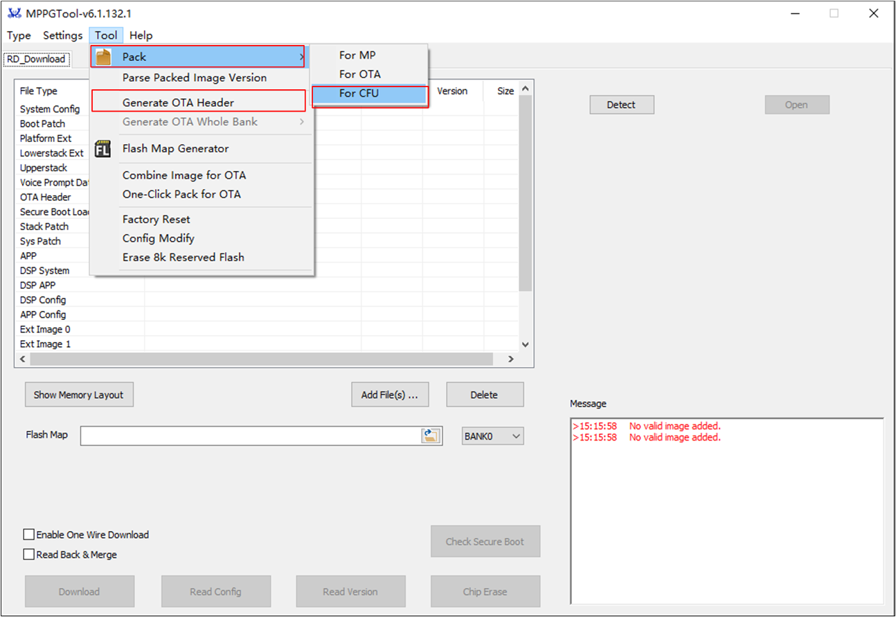
MPPG Tool
Generate OTA Header
Load flash_map.ini (e.g. RTL87X3E-SDK-VX.X.X.X\bin\flash_map_config\flash_4M\flash_map.ini) and RSA key (e.g. RTL87X3E-SDK-VX.X.X.X\tool\Gadgets\default_rsa_key.pem). Select bank0 or bank1 and fill in the version manually to generate the OTA header bin.

Generate OTA Header Image
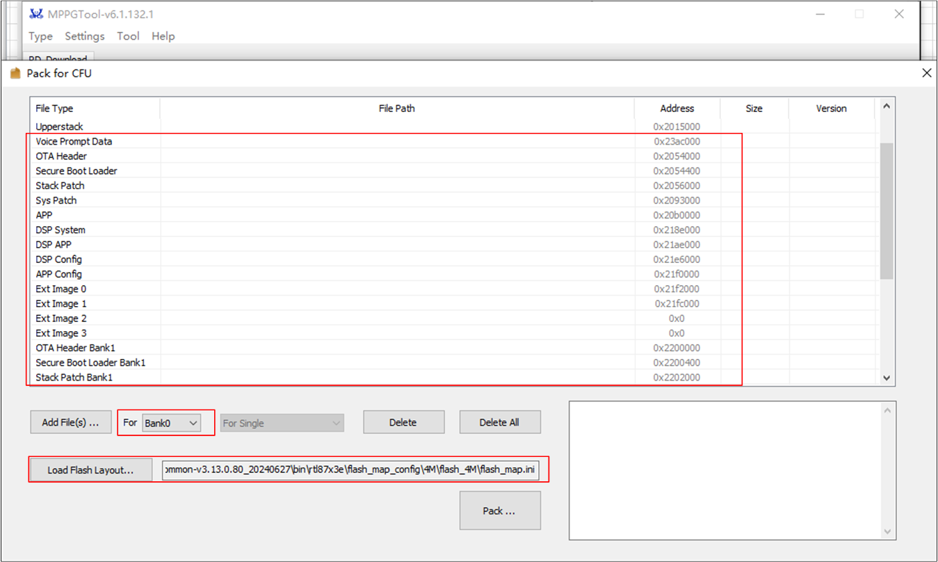
Pack Whole Images
Press Load Flash Laylout... to load
flash_map.ini(e.g.RTL87X3E-SDK-VX.X.X.X\bin\flash_map_config\flash_4M\flash_map.ini).Select and press Add File(s) to add bank0 images and optional VP image for packing bank0 images and optional VP image.
Select and press Add File(s) to add bank0 images for packing bank1 images.
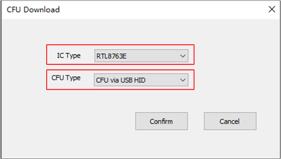
CFU Pack
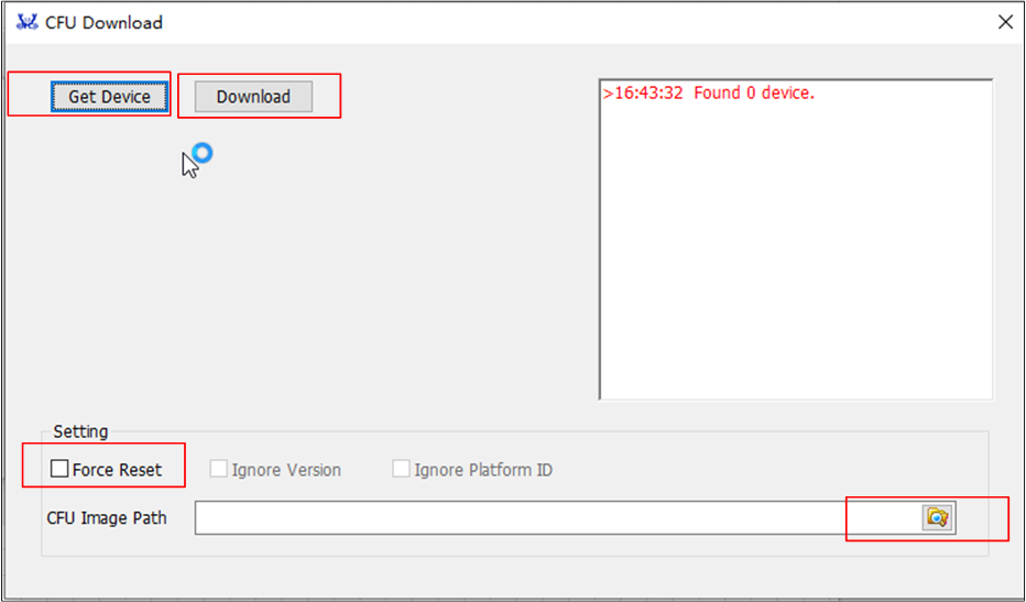
CFU Download Tool User Guide
See Also
Please refer to the relevant API Reference: