GDMA Used in DLPS
This sample illustrates the usage of GDMA in the DLPS by using UART RX GDMA.
This sample code demonstrates the communication between the chip and the PC terminal. It implements the function of receiving data via UART RX GDMA and wakes up the system using a wake-up PIN after entering DLPS mode. The system will automatically enter DLPS mode when it is idle. When data is transmitted to the chip, the wake-up PIN is first pulled low to wake up the system, allowing UART RX GDMA to continue functioning.
Users can modify some GDMA settings, including channel configuration and data transfer length, through related macro configurations. For detailed descriptions of specific macro configuration items, please refer to Configuration.
Requirements
For hardware requirements, please refer to the Requirements.
Wiring
Connect P3_1 (UART TX Pin) to the RX pin of the FT232 and P3_0 (UART RX Pin) to the TX pin of the FT232.
The hardware connection of GDMA DLPS sample code is shown in the figure below.
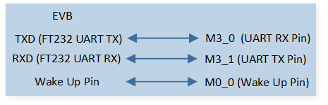
GDMA DLPS Sample Code Hardware Connection Diagram
Configurations
-
The following macros can be configured to modify the GDMA data transfer length.
#define UART_BUFFER_SIZE 1024 -
The following macros represent the parameter configurations of the allocated GDMA channel.
#define UART_RX_DMA_CHANNEL_NUM              uart_rx_dma_ch_num
#define UART_RX_DMA_CHANNEL                  DMA_CH_BASE(uart_rx_dma_ch_num)
#define UART_RX_DMA_IRQ                      DMA_CH_IRQ(uart_rx_dma_ch_num)
-
The following macros can be configured to modify UART and wake-up pin definitions.
#define WAKE_UP_PIN             P0_0
#define UART_TX_PIN             P3_1
#define UART_RX_PIN             P3_0
-
The entry function is as follows, call this function in
main()to run this sample code. For more details, please refer to the Initialization.dlps_gdma_recover_demo();
Building and Downloading
For building and downloading, please refer to the Building and Downloading.
Experimental Verification
Preparation Phase
Start a PC terminal program like PuTTY or UartAssist and connect to the used COM port with the following UART settings:
Baud rate: 3000000.
8 data bits.
1 stop bit.
No parity.
No hardware flow control.
Testing Phase
Press the Reset button on the EVB.
-
After initialization is complete, the system is in idle state, it will enter DLPS mode. Observe the entering DLPS message displayed in the Debug Analyzer.
dlps_store: enter dlps
-
Pull down the wake-up PIN to wake up the system. Observe the exiting DLPS message displayed in the Debug Analyzer.
dlps_restore: exit dlps
-
Use a PC terminal program to send data to the chip, for example, send the number 1. Once the UART receives the data, it will print the following message in the Debug Analyzer.
data_uart_handler: rx_count 1
After the data transmission is completed, the system is in idle state and will re-enter DLPS mode.
Code Overview
This section introduces the code and process description for initialization and corresponding function implementation in the sample.
Source Code Directory
The directory for project file and source code are as follows:
For project directory, please refer to Source Code Directory.
Source code directory:
sdk\src\sample\io_demo\dlps\dlps_gdma_recover_demo.c.
UART RX GDMA Initialization
The initialization flow for peripherals can refer to Initialization Flow.
-
Call
Pad_Config()andPinmux_Config()to initialize the pin.static void board_dma_uart_init(void) { Pad_Config(UART_TX_PIN, PAD_PINMUX_MODE, PAD_IS_PWRON, PAD_PULL_NONE, PAD_OUT_DISABLE, PAD_OUT_LOW); Pad_Config(UART_RX_PIN, PAD_PINMUX_MODE, PAD_IS_PWRON, PAD_PULL_UP, PAD_OUT_DISABLE, PAD_OUT_LOW); Pinmux_Config(UART_TX_PIN, UART0_TX); Pinmux_Config(UART_RX_PIN, UART0_RX); }
Call
RCC_PeriphClockCmd()to enable the UART clock and function.-
Initialize the UART peripheral:
Define the
UART_InitTypeDeftypeuartInitStruct, and callUART_StructInit()to pre-filluartInitStructwith default values.Modify the
uartInitStructparameters as needed. The UART initialization parameter configuration is shown in the table below.Call
UART_Init()to initialize the UART peripheral.
UART Initialization Parameters UART Hardware Parameters
Setting in the
uartInitStructUART
Div
1
Ovsr
8
Ovsr_adj
0x492
Parity Check
Stop Bit
Data Format
Hardware Flow Control
RX Trigger Level
29
GDMA Enable
RX Water Level
1
RX GDMA Enable
Call
UART_INTConfig()to enable uart line status interruptUART_INT_LINE_STSand RX idle timeout interruptUART_INT_IDLE.Call
NVIC_Init()to enable NVIC of UART.Call
GDMA_channel_requestto request a free GDMA channel and register the GDMA interrupt handler.Call
RCC_PeriphClockCmd()to enable the GDMA clock.-
Initialize the GDMA peripheral:
Define a
GDMA_InitTypeDeftypeGDMA_InitStruct, and callGDMA_StructInit()to pre-fillGDMA_InitStructwith default values.Modify the
GDMA_InitStructparameters as needed. The initialization parameters for the GDMA channel are configured as shown in the table below.
GDMA Initialization Parameters GDMA Hardware Parameters
Setting in the
GDMA_InitStructGDMA
Channel Num
UART_RX_DMA_CHANNEL_NUMTransfer Direction
Buffer Size
UART_BUFFER_SIZESource Address Increment or Decrement
Destination Address Increment or Decrement
Source Data Size
Destination Data Size
Source Burst Transaction Length
Destination Burst Transaction Length
Source Address
UART0->RB_THRDestination Address
uart_receive_bufSource Handshake
GDMA_Handshake_UART0_RXCall
GDMA_Init()to initialize the GDMA peripheral.Configure the GDMA total transfer completion interrupt:
GDMA_INT_Transferand NVIC. For NVIC-related configuration, refer to Interrupt Configuration.
Call
GDMA_Cmd()to enable GDMA channel for transmission.
DLPS Mode Initialization
Call
io_dlps_register()to initialize IO store/restore and do not need to worry about which IO peripheral requires specific handling.Call
power_check_cb_register()to register inquiry callback function to DLPS Framework. This function will be called each time before entering DLPS to decide whether DLPS is allowed to enter. DLPS will be disallowed if any inquiry callback function returns false. Functionuart_dlps_check_callbackwill be executed before entering DLPS:-
Call
io_dlps_register_enter_cb()to register callbacks to DLPS enter stage. Functiondlps_storewill be executed while entering DLPS:Call
Pad_PullUpOrDownValue()to configWAKE_UP_PINpull up.Call
System_WakeUpPinEnable()to to enable the wake-up function ofWAKE_UP_PIN.
-
Call
io_dlps_register_exit_cb()to register callbacks to DLPS exit stage. Functiondlps_restorewill be executed while exiting from DLPS:Set
uart_allow_enter_dlpsto false to not allow the system to enter DLPS mode.Reinitialize the GDMA peripheral.
Call
bt_power_mode_set()to set Bluetooth MAC deep sleep mode.Call
power_mode_set()to switch the system to DLPS mode.
Functional Implementation
Interrupt Handle
Pull down the wake-up PIN to wake up the system and use the PC program to send the data to the chip. When PC finishes sending data, the chip will trigger UART interrupts.
Call
UART_GetIID()to get the interrupt ID.-
If No data is received in RX idle timeout time after the RX FIFO is empty (data is received by GDMA), the
UART_FLAG_RX_IDLEinterrupt is triggered:Call
UART_GetFlagState()to checkUART_FLAG_RX_IDLEinterrupt flag state.Call
UART_INTConfig()to disableUART_INT_IDLEinterrupt.Call
GDMA_GetChannelStatus()to GDMA channel status. If channel is active, callGDMA_SuspendCmd()to suspend GDMA.Call
GDMA_GetFIFOStatus()to wait GDMA FIFO empty.Call
GDMA_GetTransferLen()to get GDMA transfer count.Call
GDMA_Cmd()to abort GDMA.Call
GDMA_SetDestinationAddress()to reconfigure the destination address of the GDMA.Call
GDMA_SuspendCmd()to resume GDMA.Call
GDMA_Cmd()to enable GDMA.Call
UART_INTConfig()to enableUART_INT_IDLEinterrupt.Set
uart_allow_enter_dlpsto true to allow the system to enter DLPS mode.