Transmit and Receive - GDMA DLPS
This sample demonstrates the functionality of sending and receiving data via CAN using GDMA in DLPS mode.
The CAN controller is connected to a USB CAN analyser and communicates with the CAN controller by sending and receiving standard data frames, extended data frames, standard remote frames, extended remote frames and other frame types through the PC side.
The SoC periodically transfers data to the PC and receives data from the PC in the CAN interrupt.
Requirements
For hardware requirements, please refer to the Requirements.
Wiring
The EVB is connected to a TJA1051 CAN Receiver module by connecting P4_0 to CTX, P4_1 to CRX. The EVB BAT/5V is connected to the module VCC and NC. The EVB GND is connected to the module GND and S.
The other end of the TJA1051 CAN Receiver module is connected to the PC via a USB CAN analyzer, by connecting module CANH to analyzer CANH and module CANL to analyzer CANL.
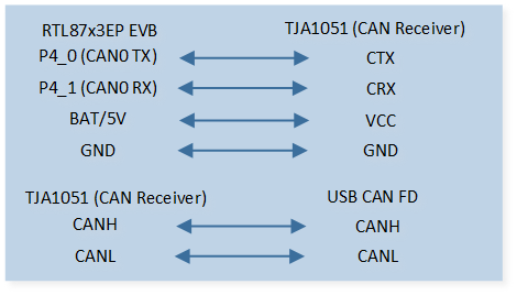
CAN TRX Demo Code Hardware Connection Diagram
The introduction of CAN transceiver can refer to CAN Transceiver Introduction .
Configurations
-
The following macros can be configured to modify CAN pin definitions.
#define CAN_TX_PIN          P4_0
#define CAN_RX_PIN          P4_1
-
The following macros can be configured to modify TX/RX message buffer ID.
#define TX_DMA_BUF_ID       3
#define RX_DMA_BUF_ID       1
-
The following macros can be used to configure the period for CAN periodic transmission and reception of data.
#define CAN_TIMER_PERIOD 5000 //ms
-
The entry function is as follows, call this function in
main()to run this sample code. For more details, please refer to the Initialization.can_trx_dma_dlps_demo();
Building and Downloading
For building and downloading, please refer to the Building and Downloading.
Experimental Verification
-
Press the Reset button on the EVB and the message will be displayed in the Debug Analyzer.
can_trx_dma_dlps_demo: start
After IC reset, every 5 seconds, CAN will send a piece of data to the PC and wait to receive a piece of data from the PC.
Use the tool to send data frames to the IC.
-
On the Debug Analyzer, print the received frame data.
dlps_store: enter dlps
dlps_restore: exit dlps
can_tx_dma_handler: TX DONE!
can_trx_handler: MB_3 tx done
can_dma_rx: waiting for rx...
can_trx_handler: CAN RX
can_trx_handler: MB_1 rx done
can_rx_dma_handler: std id = 0x00000100, ext id = 0x00000000 dlc = 8
can_rx_dma_handler: rx_data [0] 0x01
can_rx_dma_handler: rx_data [1] 0x23
can_rx_dma_handler: rx_data [2] 0x45
can_rx_dma_handler: rx_data [3] 0x67
can_rx_dma_handler: rx_data [4] 0x89
can_rx_dma_handler: rx_data [5] 0xab
can_rx_dma_handler: rx_data [6] 0xcd
can_rx_dma_handler: rx_data [7] 0xef
...
Code Overview
This section introduces the code and process description for initialization and corresponding function implementation in the sample.
Source Code Directory
The directory for project file and source code are as follows.
For project directory, please refer to Source Code Directory.
Source code directory:
sdk\sample\io_demo\canbus\dlps\can_trx_dma_dlps.c.
CAN GDMA Initialization
The initialization flow for peripherals can refer to Initialization Flow.
CAN initialization flow is shown in the following figure.
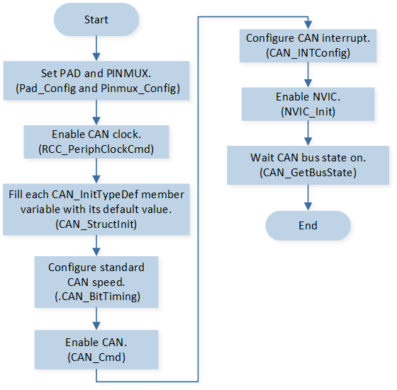
CAN Init Flow
-
Call
Pad_Config()andPinmux_Config()to configure the corresponding pin’s PAD and PINMUX.void can_board_init(void) { /* Config pinmux and pad for CAN. */ Pinmux_Config(CAN_TX_PIN, CAN_TX); Pinmux_Config(CAN_RX_PIN, CAN_RX); Pad_Config(CAN_TX_PIN, PAD_PINMUX_MODE, PAD_IS_PWRON, PAD_PULL_NONE, PAD_OUT_DISABLE, PAD_OUT_LOW); Pad_Config(CAN_RX_PIN, PAD_PINMUX_MODE, PAD_IS_PWRON, PAD_PULL_NONE, PAD_OUT_DISABLE, PAD_OUT_LOW); }
Call
RCC_PeriphClockCmd()to enable the CAN clock.-
Initialize the CAN peripheral:
Define a
CAN_InitTypeDeftypeinit_structand callCAN_StructInit()to pre-fillinit_structwith default values.Modify the
init_structparameters as needed. The CAN initialization parameters are configured as shown in the table below.Call
CAN_Init()to initialize the parameters and the CAN peripheral.
CAN Hardware Parameters |
Setting in the |
CAN |
|---|---|---|
Auto Re-transmit Enable |
||
CAN Speed Parameter - BRP |
3 |
|
CAN Speed Parameter - SJW |
3 |
|
CAN Speed Parameter - TSEG1 |
13 |
|
CAN Speed Parameter - TSEG2 |
4 |
|
RX GDMA Enable |
Call
CAN_Cmd()to enable the corresponding CAN peripheral.Call
CAN_INTConfig()to configure the CAN receive completeCAN_RX_INTinterrupt, transmit completeCAN_TX_INTinterrupt, error interruptCAN_ERROR_INT, etc. Configure NVIC, and refer to Interrupt Configuration for NVIC-related configurations.-
Call
CAN_GetBusState()to loop-check the CAN bus state and wait for the CAN bus to open.while (CAN_GetBusState() != CAN_BUS_STATE_ON) { __asm volatile ( "nop \n" ); }
Note
If the program is stuck at the point of waiting for the CAN bus to be on, please check if the CAN bus is connected correctly.
Call
GDMA_channel_requestto request a free GDMA channel and register the GDMA interrupt handler.Call
RCC_PeriphClockCmd()to enable the GDMA clock.-
Initialize the GDMA peripheral:
Define a
GDMA_InitTypeDeftypeGDMA_InitStructand executeGDMA_StructInit()to pre-fillGDMA_InitStructwith default values.Modify the
GDMA_InitStructparameters as needed. The initialization parameter configuration for GDMA TX and RX channels is shown in the following table. ExecuteGDMA_Init()to initialize the GDMA peripheral.Configure the GDMA total transfer complete interrupt
GDMA_INT_Transferand NVIC. Refer to Interrupt Configuration for related NVIC configurations.
GDMA Hardware Parameters |
Setting in the |
GDMA TX Channel |
GDMA RX Channel |
|---|---|---|---|
Channel Num |
|
|
|
Transfer Direction |
|||
Buffer Size |
|
- |
|
Source Address Increment or Decrement |
|||
Destination Address Increment or Decrement |
|||
Source Data Size |
|||
Destination Data Size |
|||
Source Burst Transaction Length |
|||
Destination Burst Transaction Length |
|||
Source Address |
- |
|
|
Destination Address |
|
- |
|
Source Handshake |
- |
||
Destination Handshake |
- |
- |
Note
During the initialization of the GDMA peripheral, do not initialize the source address of the TX GDMA channel and the destination address of the RX GDMA channel; these will be adjusted dynamically later.
DLPS Mode Initialization
Call
os_timer_create()to create a timer with a periodic interval.Call
os_timer_start()to start timer.Call
io_dlps_register()to initialize IO store/restore and do not need to worry about which IO peripheral requires specific handling.Call
power_check_cb_register()to register inquiry callback function to DLPS Framework. This function will be called each time before entering DLPS to decide whether DLPS is allowed to enter. DLPS will be disallowed if any inquiry callback function returns false. Functioncan_dlps_check_callbackwill be executed before entering DLPS.-
Call
io_dlps_register_enter_cb()to register callbacks to DLPS enter stage. Functiondlps_storewill be executed while entering DLPS.Call
Pad_Config()to configCAN_TX_PINandCAN_RX_PINpull up in order to prevent leakage.
-
Call
io_dlps_register_exit_cb()to register callbacks to DLPS exit stage. Functiondlps_restorewill be executed while exiting from DLPS.Call
Pad_Config()to configCAN_TX_PINandCAN_RX_PINpull none.Call
rx_gdma_driver_initto reinitialize the RX GDMA.Call
tx_gdma_driver_initto reinitialize the TX GDMA.
Call
bt_power_mode_set()to set Bluetooth MAC deep sleep mode.Call
power_mode_set()to switch the system to DLPS mode.
Functional Implementation
When the timer expires, the SoC will wake up from DLPS, send a piece of data to the PC, and wait to receive data from the PC.
-
The
can_timer_handlerwill be called when the timer expires.-
Call
can_start_tx_dmato send a standard data frame.Set the source address of the TX GDMA channel to the address of
tx_can_ram_struct.Enable the
GDMA_INT_Transferinterrupt for TX GDMA.Enable the GDMA peripheral to start the transmission.
Call
can_dlps_disableto disable DLPS and wait for the CAN TX to complete.
static void can_start_tx_dma(uint8_t buf_id, CAN_RAM_TypeDef *p_can_ram_data)
{
    CAN_MBTxINTConfig(CAN0, buf_id, ENABLE);

    GDMA_SetSourceAddress(TX_DMA_Channel, (uint32_t)p_can_ram_data);
    GDMA_INTConfig(TX_DMA_CHANNEL_NUM, GDMA_INT_Transfer, ENABLE);
    GDMA_Cmd(TX_DMA_CHANNEL_NUM, ENABLE);

    can_dlps_disable(APP_DLPS_ENTER_CHECK_CAN_TX(buf_id));
}
-
Call
can_dma_rxto wait for the PC to send a frame.Mask the reception of frames rtr, ide, and id filtering, i.e., receive all frames.
Enable RX GDMA and disable automatic reply.
Configure the message buffer to receive mode using the set reception frame type.
Enable message buffer reception interrupt and wait for the RAM status to be idle.
Call
can_dlps_disableto disable DLPS and wait for the PC to send data.
...
rx_frame_type.msg_buf_id = RX_DMA_BUF_ID;
rx_frame_type.frame_rtr_mask = CAN_RX_FRAME_MASK_RTR;
rx_frame_type.frame_ide_mask = CAN_RX_FRAME_MASK_IDE;
rx_frame_type.frame_id_mask = CAN_RX_FRAME_MASK_ID;
rx_frame_type.rx_dma_en = SET;
rx_frame_type.auto_reply_bit = RESET;
rx_error = CAN_SetMsgBufRxMode(CAN0, &rx_frame_type);
CAN_MBRxINTConfig(CAN0, rx_frame_type.msg_buf_id, ENABLE);
while (CAN_GetRamState(CAN0) != CAN_RAM_STATE_IDLE)
...
can_dlps_disable(APP_DLPS_ENTER_CHECK_CAN_RX(RX_DMA_BUF_ID));
-
-
After the data transmission is complete, it will enter the interrupt
can_trx_handler.Call
CAN_ClearINTPendingBit()to clear TX interrupt.Call
CAN_ClearMBnTxDoneFlag()to clear message buffer TX done flag.Call
can_dlps_enableto enable DLPS.
CAN_ClearINTPendingBit(CAN0, CAN_TX_INT_FLAG);

for (uint8_t index = 0; index < CAN_MESSAGE_BUFFER_MAX_CNT; index++)
{
    if (SET == CAN_GetMBnTxDoneFlag(CAN0, index))
    {
        IO_PRINT_INFO1("can_trx_handler: MB_%d tx done", index);
        CAN_ClearMBnTxDoneFlag(CAN0, index);

        /* Add user code. */
        can_dlps_enable(APP_DLPS_ENTER_CHECK_CAN_TX(index));
    }
}
-
When data is received, it will enter the interrupt
can_trx_handler.Call the
can_start_rx_dmafunction to enable the configuration of the GDMA buffer size, configure the destination address of the GDMA RX channel, and enable RX GDMA transmission.-
After enabling the GDMA RX channel, when CAN receives data, the GDMA transfers the data from
&(CAN0->CAN_RX_DMA_DATA)torx_dma_data_struct. When the RX GDMA reception is complete, the interrupt handler functioncan_rx_dma_handleris executed.Disable the
GDMA_INT_Transferinterrupt for RX GDMA.Call
can_dlps_enableto enable DLPS.Print the received frame ID and print the received frame data.
Clear the
GDMA_INT_Transferinterrupt flag for RX GDMA.
GDMA_INTConfig(RX_DMA_CHANNEL_NUM, GDMA_INT_Transfer, DISABLE);
can_dlps_enable(APP_DLPS_ENTER_CHECK_CAN_RX(RX_DMA_BUF_ID));
...
GDMA_ClearINTPendingBit(RX_DMA_CHANNEL_NUM, GDMA_INT_Transfer);