Output - Timer Trigger GDMA
This example introduces how to use a timer to trigger GDMA for controlling the GPIO output level.
Users can modify pin information through different macro configurations. For specific macro configurations, refer to Configurations.
Requirements
For hardware requirements, please refer to the Requirements.
Configurations
-
The following macros can be configured to modify GPIO pin definitions.
#define PIN_OUT ADC_2 -
The following macros can be configured to modify the period of GPIO level changes.
#define DMA_TIMER_INTERVAL (1000)
-
The entry function is as follows, call this function in
main()to run this sample code. For more details, please refer to the Initialization.dma_tim_demo();
Building and Downloading
For building and downloading, please refer to the Building and Downloading.
Experimental Verification
Use a logic analyzer to capture the waveform of P0_2.
Press the Reset button on the EVB.
After initialization is complete, P0_2 will output a waveform and the output waveform results of single-block or multi-block are as described below.
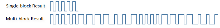
GPIO Timer Trigger GDMA Output Expected Result Diagram
Code Overview
This section introduces the code and process description for initialization and corresponding function implementation in the sample.
Source Code Directory
The directory for project file and source code are as follows.
For project directory, please refer to Source Code Directory.
Source code directory:
sdk\sample\io_demo\gdma\multiblock_tim_gpio\dma_tim_demo.c.
Initialization
The initialization flow for peripherals can refer to Initialization Flow.
-
Call
Pad_Config()andPinmux_Config()to configure the PAD and PINMUX of the corresponding pins.static void board_dma_tim_init(void) { Pad_Config(PIN_OUT, PAD_PINMUX_MODE, PAD_IS_PWRON, PAD_PULL_NONE, PAD_OUT_ENABLE, PAD_OUT_HIGH); Pinmux_Config(PIN_OUT, DWGPIO); }
Call
hw_timer_create_dma_mode()to create a hardware timer in GDMA mode.Call
RCC_PeriphClockCmd()to enable the GPIO clock.-
Initialize the GPIO peripheral.
Define the
GPIO_InitTypeDeftypeGPIO_InitStruct, and callGPIO_StructInit()to pre-fillGPIO_InitStructwith default values.Modify the
GPIO_InitStructparameters as needed. The initialization parameter configurations for GPIO are shown in the table below. CallGPIO_Init()to initialize the GPIO peripheral.
GPIO Hardware Parameters |
Setting in the |
GPIO |
|---|---|---|
GPIO Pin |
|
|
GPIO Direction |
||
GPIO Interrupt |
||
GPIO Control Mode |
Call
RCC_PeriphClockCmd()to enable the GDMA clock.Call
GDMA_channel_requestto request a free GDMA channel and register the GDMA interrupt handler.-
Initialize the GDMA peripheral:
Define a
GDMA_InitTypeDeftypeGDMA_InitStruct, and callGDMA_StructInit()to pre-fillGDMA_InitStructwith default values.Modify the
GDMA_InitStructparameters as needed. The initialization parameters for the GDMA channel are configured as shown in the table below.
GDMA Initialization Parameters GDMA Hardware Parameters
Setting in the
GDMA_InitStructGDMA
Channel Num
TIM_DMA_CHANNEL_NUMTransfer Direction
Buffer Size
10
Source Address Increment or Decrement
Destination Address Increment or Decrement
Source Data Size
Destination Data Size
Source Burst Transaction Length
Destination Burst Transaction Length
Source Address
gpio_control_patternDestination Address
GPIOA_DMA_PORT_ADDRDestination handshake
Multi-block Enable
0
Multi-block Mode
Multi-block Struct
GDMA_LLIStruct-
Configure the information of the LLI structure.
Configure
GDMA_LLIDef::SARas the source address for each block transfer, and configureGDMA_LLIDef::DARas the destination address for each block transfer.Configure
GDMA_LLIDef::LLPas a pointer to the LLI structure corresponding to the next block, to link the next transfer unit in multi-block transfers.Configure
GDMA_LLIDef::CTL_LOWwith the basic information of the GDMA transfer; refer to the sample for specific configuration.Configure
GDMA_LLIDef::CTL_HIGHwith the amount of data transferred for each block, with its value beingGDMA_InitTypeDef::GDMA_BufferSize.
for (int i = 0; i < 6; i++)
{
    if (i == 5)
    {
        //GDMA_LLIStruct[i].LLP=0;
        GDMA_LLIStruct[i].SAR = (uint32_t)(&(gpio_control_pattern_1[i]));
        GDMA_LLIStruct[i].DAR = (uint32_t)(GPIOA_DMA_PORT_ADDR);
        GDMA_LLIStruct[i].LLP = 0;  // link back to beginning
        /* configure low 32 bit of CTL register */
        GDMA_LLIStruct[i].CTL_LOW = BIT(0)
                                    | (GDMA_InitStruct.GDMA_DestinationDataSize << 1)
                                    | (GDMA_InitStruct.GDMA_SourceDataSize << 4)
                                    | (GDMA_InitStruct.GDMA_DestinationInc << 7)
                                    | (GDMA_InitStruct.GDMA_SourceInc << 9)
                                    | (GDMA_InitStruct.GDMA_DestinationMsize << 11)
                                    | (GDMA_InitStruct.GDMA_SourceMsize << 14)
                                    | (GDMA_InitStruct.GDMA_DIR << 20);
        /* configure high 32 bit of CTL register */
        GDMA_LLIStruct[i].CTL_HIGH = GDMA_InitStruct.GDMA_BufferSize;
    }
    else
    {
        GDMA_LLIStruct[i].SAR = (uint32_t)(&(gpio_control_pattern_1[i]));
        GDMA_LLIStruct[i].DAR = (uint32_t)(GPIOA_DMA_PORT_ADDR);
        GDMA_LLIStruct[i].LLP = (uint32_t)&GDMA_LLIStruct[i + 1];
        /* configure low 32 bit of CTL register */
        GDMA_LLIStruct[i].CTL_LOW = BIT(0)
                                    | (GDMA_InitStruct.GDMA_DestinationDataSize << 1)
                                    | (GDMA_InitStruct.GDMA_SourceDataSize << 4)
                                    | (GDMA_InitStruct.GDMA_DestinationInc << 7)
                                    | (GDMA_InitStruct.GDMA_SourceInc << 9)
                                    | (GDMA_InitStruct.GDMA_DestinationMsize << 11)
                                    | (GDMA_InitStruct.GDMA_SourceMsize << 14)
                                    | (GDMA_InitStruct.GDMA_DIR << 20)
                                    | BIT(28) | BIT(27);
        /* configure high 32 bit of CTL register */
        GDMA_LLIStruct[i].CTL_HIGH = GDMA_InitStruct.GDMA_BufferSize;
    }
}
Call
GDMA_Init()to initialize the GDMA peripheral.Configure the GDMA total transfer completion interrupt:
GDMA_INT_Transferand NVIC. For NVIC-related configuration, refer to Interrupt Configuration.
Call
GDMA_Cmd()to enable GDMA channel for transmission.
Functional Implementation
The array
gpio_control_patternis used to control the GPIO levels, where 1 represents a high output level, and 0 represents a low output level.Call
hw_timer_start()to start timer. Every time the timer expires twice, the GPIO level will change according to the current GDMA transfer data.When the GDMA transfer ends, the
tim_dma_handlerwill be called.