GDMA
GDMA Demo Code Support List
This chapter introduces the details of the GDMA demo code.
GDMA Demo for Memory to Memory Mode
The description of GDMA demo code 1 is shown in the following table.
Demo 1 |
|
|---|---|
Sample Purpose |
Demonstrate memory to memory by GDMA. |
Brief Introduction |
This sample code demonstrates memory to memory by GDMA. The data in |
File Path |
|
Function Entry |
|
GDMA DIR |
|
GDMA BufferSize |
100 |
GDMA SourceInc |
|
GDMA DestinationInc |
|
GDMA SourceDataSize |
|
GDMA DestinationDataSize |
|
GDMA SourceMsize |
|
GDMA DestinationMsize |
|
GDMA SourceAddr |
|
GDMA DestinationAddr |
|
Expected Result |
|
GDMA Demo for Multi-Block Mode
The description of GDMA demo code 2 is shown in the following table.
Demo 2 |
|
|---|---|
Sample Purpose |
Demonstrate how GDMA multi-block function works. |
Brief Introduction |
This sample code demonstrates how GDMA multi-block function works. The data in |
File Path |
|
Function Entry |
|
GDMA DIR |
|
GDMA BufferSize |
100 |
GDMA SourceInc |
|
GDMA DestinationInc |
|
GDMA SourceDataSize |
|
GDMA DestinationDataSize |
|
GDMA SourceMsize |
|
GDMA DestinationMsize |
|
GDMA SourceAddr |
|
GDMA DestinationAddr |
|
GDMA Multi-Block Mode |
|
Expected Result |
|
GDMA Demo for Scatter/Gather Mode
The description of GDMA demo code 3 is shown in the following table.
Demo 3 |
|
|---|---|
Sample Purpose |
Demonstrate memory to memory transfer by scatter/gather GDMA. |
Brief Introduction |
This sample code demonstrates how GDMA scatter/gather function works. The data in |
File Path |
|
Function Entry |
|
GDMA DIR |
|
GDMA BufferSize |
20 |
GDMA SourceInc |
|
GDMA DestinationInc |
|
GDMA SourceDataSize |
|
GDMA DestinationDataSize |
|
GDMA SourceMsize |
|
GDMA DestinationMsize |
|
GDMA SourceAddr |
|
GDMA DestinationAddr |
|
GDMA Scatter Mode |
|
GDMA Scatter Count |
4 |
GDMA Scatter Interval |
4 |
Expected Result |
|
UART Demo for RX Data in GDMA Mode
The description of GDMA demo code 4 is shown in the following table.
Demo 4 |
|
|---|---|
Sample Purpose |
Demonstrate how UART receives data by GDMA. |
Brief Introduction |
This sample code demonstrates the communication between chip and PC. PC transmits some data to chip. |
File Path |
|
Function Entry |
|
Hardware Connection |
As shown in GDMA Demo Code 4/5 Hardware Connection Diagram. RTL87x3E: On EVB, TX is connected to M3_0, RX is connected to M3_1, FT_VIO is connected to VIO1, and CON3 is connected to PC. RTL87x3D: On EVB, TXD is connected to M3_0, RXD is connected to M3_1, FT_VIO is connected to VIO1, and P2 is connected to PC. |
UART TX Pin Definition |
|
UART RX Pin Definition |
|
UART ID |
UART0 |
Baud Rate |
3000000 |
Parity Check |
No parity |
Data Format |
8-Bit |
Stop Bit |
1-Bit |
Hardware Flow Control |
None |
Expected Result |
|
The hardware connection of GDMA demo code 4 is shown in the figure below.

GDMA Demo Code 4/5 Hardware Connection Diagram
UART Demo for TX Data in GDMA Mode
The description of GDMA demo code 5 is shown in the following table.
Demo 5 |
|
|---|---|
Sample Purpose |
Demonstrate how UART sends data by GDMA. |
Brief Introduction |
This sample code demonstrates the communication between chip and PC. Chip transmits some data to PC. |
File Path |
|
Function Entry |
|
Hardware Connection |
As shown in GDMA Demo Code 4/5 Hardware Connection Diagram. RTL87x3E: On EVB, TX is connected to M3_0, RX is connected to M3_1, FT_VIO is connected to VIO1, and CON3 is connected to PC. RTL87x3D: On EVB, TXD is connected to M3_0, RXD is connected to M3_1, FT_VIO is connected to VIO1, and P2 is connected to PC. |
UART TX Pin Definition |
|
UART RX Pin Definition |
|
UART ID |
UART0 |
Baud Rate |
115200 |
Parity Check |
No parity |
Data Format |
8-Bit |
Stop Bit |
1-Bit |
Hardware Flow Control |
None |
Expected Result |
Press the Reset button on the EVB, string ### Welcome to use RealTek Bumblebee ###\r\n will be displayed in UART debug tool. |
ADC Demo for GDMA Mode
The description of GDMA demo code 6 is shown in the following table.
Demo 6 |
|
|---|---|
Sample Purpose |
Demonstrate how ADC samples data in continuous mode by GDMA. |
Brief Introduction |
Use continuous mode of ADC peripheral to measure voltage on P0_0 and P0_1. |
File Path |
|
Function Entry |
|
Pre-Condition |
Turn off Charger auto enable and Battery detection support on the MCUConfig Tool. |
Channel |
ADC0 ADC1 |
External Channel Input Mode |
ADC0 and ADC1 are divide mode. |
Hardware Connection |
Connect M0_0 and M0_1 of EVB to external DC voltage source. Input voltage of M0_0 and M0_1 must range from 0 to 3.3V. |
Expected Result |
Press the Reset button on the EVB, ADC starts continuous sampling, and sample rawdata will be stored
in array |
I2C Demo for GDMA Mode
The description of GDMA demo code 7 is shown in the following table.
Demo 7 |
|
|---|---|
Sample Purpose |
Demonstrate how I2C master and slave work in GDMA mode. |
Brief Introduction |
This sample code demonstrates the communication between I2C master and slave in GDMA mode. Master will read data from slave. |
File Path |
|
Function Entry |
|
Hardware Connection |
As shown in GDMA Demo Code 7 Hardware Connection Diagram. On EVB, connect P0_0 to P1_0, connect P0_1 to P1_1. |
I2C Master SCL Pin Definition |
|
I2C Master SDA Pin Definition |
|
I2C Slave SCL Pin Definition |
|
I2C Slave SDA Pin Definition |
|
I2C Master ID |
I2C1 |
I2C Slave ID |
I2C0 |
Clock Speed |
400000 |
Address Mode |
7-Bit |
Slave Address |
0x50 |
ACK |
ACK enable |
GDMA DIR |
Master: Slave: |
GDMA BufferSize |
|
GDMA SourceInc |
Master: Slave: |
GDMA DestinationInc |
Master: Slave: |
GDMA SourceDataSize |
Master: Slave: |
GDMA DestinationDataSize |
Master: Slave: |
GDMA SourceMsize |
|
GDMA DestinationMsize |
|
GDMA SourceAddr |
Master: Slave: |
GDMA DestinationAddr |
Master: Slave: |
GDMA SourceHandshake |
Master: |
GDMA DestHandshake |
Slave: |
Expected Result |
|
The hardware connection of GDMA demo code 7 is shown in the figure below.
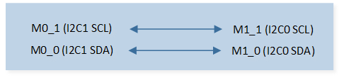
GDMA Demo Code 7 Hardware Connection Diagram
GDMA Demo for DLPS Recover
The description of GDMA demo code 8 is shown in the following table.
Demo 8 |
|
|---|---|
Sample Purpose |
Demonstrate how GDMA recovers from DLPS. |
Brief Introduction |
This sample code demonstrates how GDMA recovers from DLPS. The UART can receive data through GDMA when the chip wakes up from DLPS. |
File Path |
|
Function Entry |
|
Hardware Connection |
As shown in GDMA Demo Code 8 Hardware Connection Diagram. RTL87x3E: On EVB, TX is connected to M3_0, RX is connected to M3_1, FT_VIO is connected to VIO1, CON3 is connected to PC, and wake up pin is connected to P0_0. RTL87x3D: On EVB, TXD is connected to M3_0, RXD is connected to M3_1, FT_VIO is connected to VIO1, P2 is connected to PC, and wake up pin is connected to P0_0. |
UART TX Pin Definition |
|
UART RX Pin Definition |
|
UART ID |
UART0 |
Baud Rate |
3000000 |
Parity Check |
No parity |
Data Format |
8-Bit |
Stop Bit |
1-Bit |
Hardware Flow Control |
None |
Expected Result |
|
The hardware connection of GDMA demo code 8 is shown in the figure below.
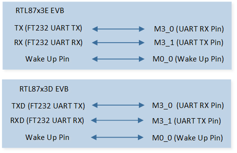
GDMA Demo Code 8 Hardware Connection Diagram
SPI Demo for GDMA Mode
The description of GDMA demo code 9 is shown in the following table.
Demo 9 |
|
|---|---|
Sample Purpose |
Demonstrate how SPI sends and receives data in master mode by GDMA. |
File Path |
|
Function Entry |
|
Hardware Connection |
As shown in GDMA Demo Code 9 Hardware Connection Diagram. Connect M0_1 to CS of SPI slave device, connect M0_0 to SCK of SPI slave device, connect M1_0 to MISO of SPI slave device, and connect M1_1 to MOSI of SPI slave device. |
SPI CS Pin Definition |
|
SPI SCK Pin Definition |
|
SPI MOSI Pin Definition |
|
SPI MISO Pin Definition |
|
SPI ID |
SPI1 |
Mode |
Master |
Speed |
400000 |
Data Size |
8-Bit |
Expected Result |
|
The hardware connection of GDMA demo code 9 is shown in the figure below.
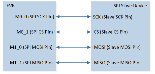
GDMA Demo Code 9 Hardware Connection Diagram
Functional Overview
GDMA is used to provide high-speed data transfer between peripherals and memory or between memory and memory. The data transfer can be done independently of the CPU to reduce the CPU overhead.
Each channel of the GDMA controller can handle requests from one or more peripherals for memory access. The GDMA controller has an arbitrator to coordinate the priority of each GDMA request.
Feature List
Programmable transfer type for each channel: memory to memory, memory to peripheral, peripheral to memory, peripheral to peripheral.
Programmable source and destination addresses for each channel.
Address increment, or fixed.
Programmable burst transaction size for each channel.
Support transfer abort/suspend function.
Programmable channel priority.
Independent interrupts and control bit for every channel.
Support single-block and multi-block transfer.
Support scatter and gather transfer.
Note
RTL87x3D supports 16 channels, if using SPI high-speed mode, please use channel 0 and 1. RTL87x3E supports 9 channels, RTL87x3EP supports 12 channels.
Parameter Significance
GDMA_ChannelNumChannel numbers can be 0 to 15.
GDMA_DIRThe transfer direction can be memory to memory or memory to peripheral or peripheral to memory or peripheral to peripheral.
GDMA_SourceIncIndicates whether to increment the source address on every source transfer.
GDMA_DestinationIncIndicates whether to increment the destination address on every destination transfer.
GDMA_SourceDataSizeSource single transaction size in bytes: src_single_size_bytes =
GDMA_SourceDataSizeGDMA_DestinationDataSizeDestination single transaction size in bytes: dst_single_size_bytes =
GDMA_DestinationDataSizeGDMA_SourceMsizeSource burst transaction size in bytes: src_burst_size_bytes =
GDMA_SourceMsize* src_single_size_bytesGDMA_DestinationMsizeDestination burst transaction size in bytes: dst_burst_size_bytes =
GDMA_DestinationMsize* dst_single_size_bytesGDMA_BufferSizeThe total number of bytes to be transferred in a block is: blk_size_bytes_dma =
GDMA_BufferSize* src_single_size_bytes
Note
GDMA_SourceDataSize * GDMA_SourceMsize = GDMA_DestinationDataSize * GDMA_DestinationMsizeWaterlevel Setting
Handshaking interfaces are used at the transaction level to control the flow of single or burst transactions. Waterlevel is mainly divided into TX FIFO waterlevel and RX FIFO waterlevel. When the effective data amount in the FIFO reaches the set value of waterlevel, a burst transmission is initiated. GDMA_SourceMsize, GDMA_DestinationMsize, GDMA_SourceDataSize, GDMA_DestinationDataSize and peripheral waterlevel setting table is presented below.
Dir |
Peripheral GDMA waterlevel |
GDMA_SourceMsize |
GDMA_DestinationMsize |
GDMA_SourceDataSize |
GDMA_DestinationDataSize |
|
|---|---|---|---|---|---|---|
UART |
TX |
|
1 |
4 |
Word |
Byte |
RX |
|
4 |
1 |
Byte |
Word |
|
SPI Master |
TX |
|
4 |
8 |
Word |
HalfWord |
RX |
|
8 |
4 |
HalfWord |
Word |
|
TX |
|
1 |
4 |
Word |
Byte |
|
RX |
|
4 |
1 |
Byte |
Word |
|
SPI Slave |
TX |
|
1 |
4 |
Word |
Byte |
RX |
|
4 |
1 |
Byte |
Word |
|
I2C |
TX |
|
4 |
8 |
Word |
HalfWord |
RX |
|
4 |
1 |
Byte |
Word |
|
ADC |
|
8 |
8 |
HalfWord |
HalfWord |
|
SPI_HS |
TX |
|
32 |
32 |
Byte |
Byte |
RX |
|
32 |
32 |
Byte |
Byte |
Program Examples
Single-Block Transfer Initialization Flow
The initialization flow of GDMA single-block transfer is shown in the following figure.
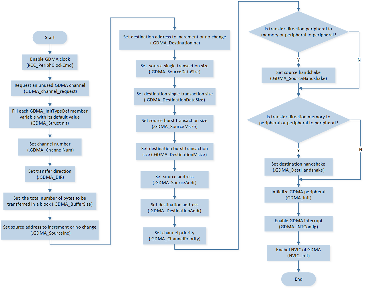
GDMA Single-Block Transfer Operation Flow Chart
The codes below demonstrate the GDMA single-block transfer.
uint16_t i = 0;
RCC_PeriphClockCmd(APBPeriph_GDMA, APBPeriph_GDMA_CLOCK, ENABLE);
GDMA_InitTypeDef GDMA_InitStruct;

if (!GDMA_channel_request(&mem_to_mem_dma_ch_num, demo_dma_handler, true))
{
   return;
}

/*--------------initialize test buffer---------------------*/
for (i = 0; i < 100; i++)
{
   GDMA_SendBuffer[i] = (i & 0xff);
}
for (i = 0; i < 100; i++)
{
   GDMA_RecvBuffer[i] = 0;
}

GDMA_StructInit(&GDMA_InitStruct);
GDMA_InitStruct.GDMA_ChannelNum      = DEMO_DMA_CHANNEL_NUM;
GDMA_InitStruct.GDMA_DIR             = GDMA_DIR_MemoryToMemory;
GDMA_InitStruct.GDMA_BufferSize      = 100;//determine total transfer size
GDMA_InitStruct.GDMA_SourceInc       = DMA_SourceInc_Inc;
GDMA_InitStruct.GDMA_DestinationInc  = DMA_DestinationInc_Inc;
GDMA_InitStruct.GDMA_SourceDataSize  = GDMA_DataSize_Byte;
GDMA_InitStruct.GDMA_DestinationDataSize = GDMA_DataSize_Byte;
GDMA_InitStruct.GDMA_SourceMsize      = GDMA_Msize_1;
GDMA_InitStruct.GDMA_DestinationMsize = GDMA_Msize_1;
GDMA_InitStruct.GDMA_SourceAddr      = (uint32_t)GDMA_SendBuffer;
GDMA_InitStruct.GDMA_DestinationAddr = (uint32_t)GDMA_RecvBuffer;
GDMA_Init(DEMO_DMA_CHANNEL, &GDMA_InitStruct);

/*-----------------GDMA IRQ init-------------------*/
NVIC_InitTypeDef nvic_init_struct;
nvic_init_struct.NVIC_IRQChannel         = DEMO_DMA_IRQ;
nvic_init_struct.NVIC_IRQChannelCmd      = (FunctionalState)ENABLE;
nvic_init_struct.NVIC_IRQChannelPriority = 3;
NVIC_Init(&nvic_init_struct);

GDMA_INTConfig(DEMO_DMA_CHANNEL_NUM, GDMA_INT_Block, ENABLE);
GDMA_Cmd(DEMO_DMA_CHANNEL_NUM, ENABLE);