SPI
SPI Demo Code Support List
This chapter introduces the details of the SPI demo code.
SPI Demo For Switch CS Signals
The description of SPI demo code 1 is shown in the following table.
Demo 1 |
|
|---|---|
Sample Purpose |
Demonstrate how SPI dynamically switches CS signals. |
File Path |
|
Function Entry |
|
Hardware Connection |
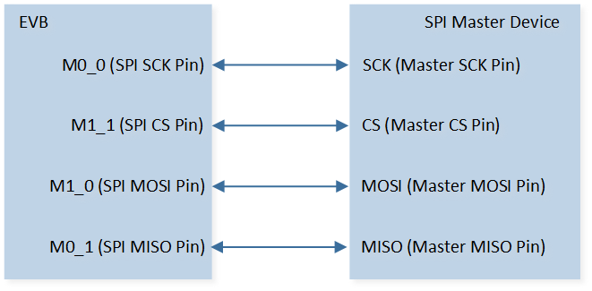
As shown in SPI Demo Code 1 Hardware Connection Diagram. Connect M1_3 to CS of SPI slave device 0, connect M1_4 to CS of SPI slave device 1, connect M1_5 to CS of SPI slave device 2, connect M1_0 to SCK of SPI slave device 0/1/2, connect M1_1 to MISO of SPI slave device 0/1/2, and connect M1_2 to MOSI of SPI slave device 0/1/2. |
SPI CS0 Pin Definition |
|
SPI CS1 Pin Definition |
|
SPI CS2 Pin Definition |
|
SPI SCK Pin Definition |
|
SPI MOSI Pin Definition |
|
SPI MISO Pin Definition |
|
SPI ID |
SPI1 |
Mode |
Master |
Speed |
400000 |
Data Size |
8-Bit |
Expected Result |
|
The hardware connection of SPI demo code 1 is shown in the figure below.
SPI Demo Code 1 Hardware Connection Diagram
SPI Demo for EEPROM Mode
The description of SPI demo code 2 is shown in the following table.
Demo 2 |
|
|---|---|
Sample Purpose |
Demonstrate how SPI receives data with EEPROM mode by GDMA in master mode. |
File Path |
|
Function Entry |
|
Hardware Connection |
As shown in SPI Demo Code 2/6 Hardware Connection Diagram. Connect M0_3 to CS of SPI slave device, connect M0_0 to SCK of SPI slave device, connect M0_1 to MISO of SPI slave device, and connect M0_2 to MOSI of SPI slave device. |
SPI CS Pin Definition |
|
SPI SCK Pin Definition |
|
SPI MOSI Pin Definition |
|
SPI MISO Pin Definition |
|
SPI ID |
SPI1 |
Mode |
Master |
Speed |
400000 |
Data Size |
8-Bit |
Expected Result |
Print string spi_master_rx_dma_handler and the received data in Debug Analyzer. |
The hardware connection of SPI demo code 2 is shown in the figure below.
SPI Demo Code 2/6 Hardware Connection Diagram
SPI Demo for External Flash
The description of SPI demo code 3 is shown in the following table.
Demo 3 |
|
|---|---|
Sample Purpose |
Demonstrate how the chip communicates with external flash by SPI. |
File Path |
|
Function Entry |
|
Hardware Connection |
As shown in SPI Demo Code 3 Hardware Connection Diagram. Connect M5_1 to CS of external flash, connect M5_0 to SCK of external flash, connect M5_3 to MISO of external flash, and connect M5_2 to MOSI of external flash, connect M5_5 to HOLD of external flash. |
SPI CS Pin Definition |
|
SPI SCK Pin Definition |
|
SPI MOSI Pin Definition |
|
SPI MISO Pin Definition |
|
FLASH HOLD Pin Definition |
|
SPI ID |
SPI0 |
Mode |
Master |
Speed |
400000 |
Data Size |
8-Bit |
Expected Result |
|
The hardware connection of SPI demo code 3 is shown in the figure below.
SPI Demo Code 3 Hardware Connection Diagram
SPI Demo for Interrupt Mode
The description of SPI demo code 4 is shown in the following table.
Demo 4 |
|
|---|---|
Sample Purpose |
Demonstrate how SPI sends data by polling and receives data by interrupt in master mode. |
File Path |
|
Function Entry |
|
Hardware Connection |
As shown in SPI Demo Code 4 Hardware Connection Diagram. Connect M0_1 to CS of SPI slave device, connect M0_0 to SCK of SPI slave device, connect M1_0 to MISO of SPI slave device, and connect M1_1 to MOSI of SPI slave device. |
SPI CS Pin Definition |
|
SPI SCK Pin Definition |
|
SPI MOSI Pin Definition |
|
SPI MISO Pin Definition |
|
SPI ID |
SPI1 |
Mode |
Master |
Speed |
400000 |
Data Size |
8-Bit |
Expected Result |
|
The hardware connection of SPI demo code 4 is shown in the figure below.
SPI Demo Code 4 Hardware Connection Diagram
SPI Demo for Polling Mode
The description of SPI demo code 5 is shown in the following table.
Demo 5 |
|
|---|---|
Sample Purpose |
Demonstrate how SPI sends and receives data by polling in master mode. |
File Path |
|
Function Entry |
|
Hardware Connection |
As shown in SPI Demo Code 5 Hardware Connection Diagram. Connect M1_5 to CS of SPI slave device, connect M1_2 to SCK of SPI slave device, connect M1_3 to MISO of SPI slave device, and connect M1_4 to MOSI of SPI slave device. |
SPI CS Pin Definition |
|
SPI SCK Pin Definition |
|
SPI MOSI Pin Definition |
|
SPI MISO Pin Definition |
|
SPI ID |
SPI1 |
Mode |
Master |
Speed |
400000 |
Data Size |
8-Bit |
Expected Result |
|
The hardware connection of SPI demo code 5 is shown in the figure below.
SPI Demo Code 5 Hardware Connection Diagram
SPI Demo for RX Only Mode
The description of SPI demo code 6 is shown in the following table.
Demo 6 |
|
|---|---|
Sample Purpose |
Demonstrate how SPI receives data with receive only mode by GDMA in master mode. |
File Path |
|
Function Entry |
|
Hardware Connection |
As shown in SPI Demo Code 2/6 Hardware Connection Diagram. Connect M0_3 to CS of SPI slave device, connect M0_0 to SCK of SPI slave device, connect M0_1 to MISO of SPI slave device, and connect M0_2 to MOSI of SPI slave device. |
SPI CS Pin Definition |
|
SPI SCK Pin Definition |
|
SPI MOSI Pin Definition |
|
SPI MISO Pin Definition |
|
SPI ID |
SPI1 |
Mode |
Master |
Speed |
400000 |
Data Size |
8-Bit |
Expected Result |
Print string spi_master_rx_dma_handler and the received data in Debug Analyzer. |
SPI Demo for RX Data in Slave Mode
The description of SPI demo code 7 is shown in the following table.
Demo 7 |
|
|---|---|
Sample Purpose |
Demonstrate how SPI receives data by interrupt in slave mode. |
File Path |
|
Function Entry |
|
Hardware Connection |
As shown in SPI Demo Code 7 Hardware Connection Diagram. Connect MIC2_N to CS of SPI master device, connect MIC1_P to SCK of SPI master device, connect MIC2_P to MISO of SPI master device, and connect MIC1_N to MOSI of SPI master device. |
SPI CS Pin Definition |
|
SPI SCK Pin Definition |
|
SPI MOSI Pin Definition |
|
SPI MISO Pin Definition |
|
SPI ID |
SPI0 |
Mode |
Slave |
Data Size |
8-Bit |
Expected Result |
Master device sends data to the chip. The chip stores the received data in array |
The hardware connection of SPI demo code 7 is shown in the figure below.
SPI Demo Code 7 Hardware Connection Diagram
SPI Demo for TX Data in Slave Mode
The description of SPI demo code 8 is shown in the following table.
Demo 8 |
|
|---|---|
Sample Purpose |
Demonstrate how SPI sends data in slave mode by interrupt. |
File Path |
|
Function Entry |
|
Hardware Connection |
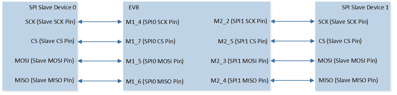
As shown in SPI Demo Code 8 Hardware Connection Diagram. Connect M1_4 to M1_0, connect M1_7 to M1_3, connect M1_5 to M1_2, connect M1_6 to M1_1, and connect M2_3 to M2_4. |
SPI0 CS Pin Definition |
|
SPI0 SCK Pin Definition |
|
SPI0 MOSI Pin Definition |
|
SPI0 MISO Pin Definition |
|
SPI1 CS Pin Definition |
|
SPI1 SCK Pin Definition |
|
SPI1 MOSI Pin Definition |
|
SPI1 MISO Pin Definition |
|
SPI ID |
SPI0 SPI1 |
Mode |
SPI1 is master, SPI0 is slave. |
Speed |
100000 |
Data Size |
8-Bit |
Expected Result |
|
The hardware connection of SPI demo code 8 is shown in the figure below.
SPI Demo Code 8 Hardware Connection Diagram
SPI Demo for GDMA Mode in Slave Mode
The description of SPI demo code 9 is shown in the following table.
Demo 9 |
|
|---|---|
Sample Purpose |
Demonstrate how SPI sends data in slave mode by GDMA. |
File Path |
|
Function Entry |
|
Hardware Connection |
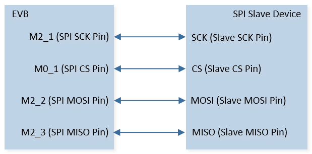
As shown in SPI Demo Code 9 Hardware Connection Diagram. Connect M2_2 to CS of SPI master device, connect M1_0 to SCK of SPI master device, connect M1_1 to MISO of SPI master device, and connect M2_1 to MOSI of SPI master device. |
SPI CS Pin Definition |
|
SPI SCK Pin Definition |
|
SPI MOSI Pin Definition |
|
SPI MISO Pin Definition |
|
SPI ID |
SPI0 |
Mode |
Slave |
Data Size |
8-Bit |
Expected Result |
|
The hardware connection of SPI demo code 9 is shown in the figure below.

SPI Demo Code 9 Hardware Connection Diagram
SPI Demo for High-Speed Mode in Master Mode
The description of SPI demo code 10 is shown in the following table.
Demo 10 |
|
|---|---|
Sample Purpose |
Demonstrate how SPI0 sends and receives data in high-speed mode. |
File Path |
|
Function Entry |
|
Hardware Connection |
As shown in SPI Demo Code 10 Hardware Connection Diagram. Connect M1_2 to CS of SPI slave device, connect M1_3 to SCK of SPI slave device, connect M1_4 to MISO of SPI slave device, and connect M1_5 to MOSI of SPI slave device. |
SPI CS Pin Definition |
|
SPI SCK Pin Definition |
|
SPI MOSI Pin Definition |
|
SPI MISO Pin Definition |
|
SPI ID |
SPI0 |
Mode |
Master |
Speed |
40MHz |
Data Size |
8-Bit |
Expected Result |
|
The hardware connection of SPI demo code 10 is shown in the figure below.
SPI Demo Code 10 Hardware Connection Diagram
SPI Demo for SPI0 and SPI1 Communication by GDMA Mode
The description of SPI demo code 11 is shown in the following table.
Demo 11 |
|
|---|---|
Sample Purpose |
Demonstrate how SPI0 reads data and SPI1 sends data by GDMA. |
File Path |
|
Function Entry |
|
Hardware Connection |
As shown in SPI Demo Code 11/12 Hardware Connection Diagram. Connect M1_7 to CS of SPI slave device 0, connect M1_4 to SCK of SPI slave device 0, connect M1_5 to MISO of SPI slave device 0, and connect M1_6 to MOSI of SPI slave device 0. Connect M2_5 to CS of SPI slave device 1, connect M2_2 to SCK of SPI slave device 1, connect M2_3 to MISO of SPI slave device 1, and connect M2_4 to MOSI of SPI slave device 1. |
SPI0 CS Pin Definition |
|
SPI0 SCK Pin Definition |
|
SPI0 MOSI Pin Definition |
|
SPI0 MISO Pin Definition |
|
SPI1 CS Pin Definition |
|
SPI1 SCK Pin Definition |
|
SPI1 MOSI Pin Definition |
|
SPI1 MISO Pin Definition |
|
SPI ID |
SPI0 SPI1 |
Mode |
Master |
Speed |
400000 |
Data Size |
8-Bit |
Expected Result |
SPI0 reads data from SPI slave device 0 and SPI1 sends the same data to SPI slave device 1. |
The hardware connection of SPI demo code 11 is shown in the figure below.
SPI Demo Code 11/12 Hardware Connection Diagram
SPI Demo for SPI0 and SPI1 Communication by Auto-Reload GDMA Mode
The description of SPI demo code 12 is shown in the following table.
Demo 12 |
|
|---|---|
Sample Purpose |
Demonstrate how SPI0 reads data and SPI1 sends data by auto-reload GDMA. |
File Path |
|
Function Entry |
|
Hardware Connection |
As shown in SPI Demo Code 11/12 Hardware Connection Diagram. Connect M1_7 to CS of SPI slave device 0, connect M1_4 to SCK of SPI slave device 0, connect M1_5 to MISO of SPI slave device 0, and connect M1_6 to MOSI of SPI slave device 0. Connect M2_5 to CS of SPI slave device 1, connect M2_2 to SCK of SPI slave device 1, connect M2_3 to MISO of SPI slave device 1, and connect M2_4 to MOSI of SPI slave device 1. |
SPI0 CS Pin Definition |
|
SPI0 SCK Pin Definition |
|
SPI0 MOSI Pin Definition |
|
SPI0 MISO Pin Definition |
|
SPI1 CS Pin Definition |
|
SPI1 SCK Pin Definition |
|
SPI1 MOSI Pin Definition |
|
SPI1 MISO Pin Definition |
|
SPI ID |
SPI0 SPI1 |
Mode |
Master |
Speed |
400000 |
Data Size |
8-Bit |
Expected Result |
SPI0 reads data from SPI slave device 0 and SPI1 sends the same data to SPI slave device 1. |
SPI Demo for RX Data at High-Speed Mode in Slave Mode
The description of SPI demo code 13 is shown in the following table.
Demo 13 |
|
|---|---|
Sample Purpose |
Demonstrate how SPI0 slave reads data at high speed in GDMA mode. |
File Path |
|
Function Entry |
|
Hardware Connection |
As shown in SPI Demo Code 13/14 Hardware Connection Diagram. Connect M1_1 to the CS of the SPI master device, connect M0_0 to the SCK of the SPI master device, connect M0_1 to the MISO of the SPI master device, and connect M1_0 to the MOSI of the SPI master device. |
SPI CS Pin Definition |
|
SPI SCK Pin Definition |
|
SPI MOSI Pin Definition |
|
SPI MISO Pin Definition |
|
SPI ID |
SPI0 |
Mode |
Slave |
Speed |
10MHz |
Data Size |
8-Bit |
Expected Result |
Print the string spi_slave_rx_dma_handler! rx_len_all 1000 and the received data in Debug Analyzer. |
The hardware connection of SPI demo code 13 is shown in the figure below.
SPI Demo Code 13/14 Hardware Connection Diagram
SPI Demo for TX Data at High-Speed Mode in Slave Mode
The description of SPI demo code 14 is shown in the following table.
Demo 14 |
|
|---|---|
Sample Purpose |
Demonstrate how SPI0 slave sends data at high speed in GDMA mode. |
File Path |
|
Function Entry |
|
Hardware Connection |
As shown in SPI Demo Code 13/14 Hardware Connection Diagram. Connect M1_1 to the CS of the SPI master device, connect M0_0 to the SCK of the SPI master device, connect M0_1 to the MISO of the SPI master device, and connect M1_0 to the MOSI of the SPI master device. |
SPI CS Pin Definition |
|
SPI SCK Pin Definition |
|
SPI MOSI Pin Definition |
|
SPI MISO Pin Definition |
|
SPI ID |
SPI0 |
Mode |
Slave |
Speed |
10MHz |
Data Size |
8-Bit |
Expected Result |
The data in the array |
SPI Demo for Controlling LED in Polling Mode
The description of SPI demo code 15 is shown in the following table.
Demo 15 |
|
|---|---|
Sample Purpose |
Demonstrate how SPI1 uses one data line to control the LED in polling mode. |
File Path |
|
Function Entry |
|
Hardware Connection |
Connect M1_0 to the LED controller. |
SPI MOSI Pin Definition |
|
SPI ID |
SPI1 |
Mode |
Master |
Speed |
10MHz |
Data Size |
8-Bit |
Expected Result |
Press the Reset button on the EVB, the data in the array |
SPI Demo for Controlling LED in Interrupt Mode
The description of SPI demo code 16 is shown in the following table.
Demo 16 |
|
|---|---|
Sample Purpose |
Demonstrate how SPI1 uses one data line to control the LED in interrupt mode. |
File Path |
|
Function Entry |
|
Hardware Connection |
Connect M1_0 to the LED controller. |
SPI MOSI Pin Definition |
|
SPI ID |
SPI1 |
Mode |
Master |
Speed |
10MHz |
Data Size |
8-Bit |
Expected Result |
Press the Reset button on the EVB, the data in the array |
SPI Demo for Controlling LED in GDMA Mode
The description of SPI demo code 17 is shown in the following table.
Demo 17 |
|
|---|---|
Sample Purpose |
Demonstrate how SPI1 uses one data line to control the LED in GDMA mode. |
File Path |
|
Function Entry |
|
Hardware Connection |
Connect M1_0 to the LED controller. |
SPI MOSI Pin Definition |
|
SPI ID |
SPI1 |
Mode |
Master |
Speed |
10MHz |
Data Size |
8-Bit |
Expected Result |
Press the Reset button on the EVB, the data in the array |
SPI Demo for TX Data Using GDMA Mode in DLPS Situation as Master
The description of SPI demo code 18 is shown in the following table.
Demo 18 |
|
|---|---|
Sample Purpose |
Demonstrate how SPI master sends data by GDMA mode in DLPS situation. |
File Path |
|
Function Entry |
|
Hardware Connection |
As shown in SPI Demo Code 18 Hardware Connection Diagram. Connect M0_1 to CS of SPI slave device, connect M2_1 to SCK of SPI slave device, connect M2_3 to MISO of SPI slave device, and connect M2_2 to MOSI of SPI slave device. |
SPI CS Pin Definition |
|
SPI SCK Pin Definition |
|
SPI MOSI Pin Definition |
|
SPI MISO Pin Definition |
|
SPI ID |
SPI0 |
Mode |
Master |
Data Size |
8-Bit |
Expected Result |
The device enters DLPS, and after being awakened by the timer every 1 second, the data in the array |
The hardware connection of SPI demo code 18 is shown in the figure below.
SPI Demo Code 18 Hardware Connection Diagram
Functional Overview
SPI allows the chip to communicate with external devices in half/full duplex, synchronous, and serial modes.
Feature List
Support master and slave modes.
Support 4-bit to 32-bit data size in master mode.
Support 4-bit to 16-bit data size in slave mode.
Support up to 3 slave devices in master mode.
Support GDMA.
The maximum SPI clock supported by SPI in master mode and slave mode is as follows.
IC Type |
SPI0 Master Max Clock (MHz) |
SPI1 Master Max Clock (MHz) |
SPI2 Master Max Clock (MHz) |
SPI0 Slave Max Clock (MHz) |
|---|---|---|---|---|
50 (with dedicated I/Os) 10 (with general I/Os) |
20 (with dedicated I/Os) 10 (with general I/Os) |
20 (with dedicated I/Os) 10 (with general I/Os) |
10 |
|
50 (with dedicated I/Os) 10 (with general I/Os) |
20 (with dedicated I/Os) 10 (with general I/Os) |
20 (with dedicated I/Os) 10 (with general I/Os) |
10 |
|
40 (with dedicated I/Os) 10 (with general I/Os) |
20 (with dedicated I/Os) 10 (with general I/Os) |
20 (with dedicated I/Os) 10 (with general I/Os) |
10 |
Note
RTL87x3D, RTL87x3E, and RTL87x3EP support 3 SPI. SPI0 supports master mode and slave mode. SPI1 and SPI2 only support master mode.
SPI0 and SPI1 support 3 slave devices in master mode, and SPI2 supports 1 slave device in master mode.
If the user needs to operate flash and read data from flash, it is recommended to use
SPI_Direction_EEPROMmode. In this mode, the SPI controller will automatically supplement the padding bits needed for reading back. Set the read data length bySPI_SetReadLen()before reading from flash, then the result ofSPI_GetRxFIFOLen()will equal this value. IfSPI_Direction_FullDuplexmode is used when operating flash, it needs to supplement the padding bits manually, and the number of bytes should be equal to the read data length. In this way, the result ofSPI_GetRxFIFOLen()is the total length of padding bits and data to read.SPI_SetReadLen()is just forSPI_Direction_EEPROMmode.SPI support up to 50MHz (SPI0 of RTL87x3E and RTL87x3EP), 40MHz (SPI0 of RTL87x3D) and 20MHz (SPI1 and SPI2) with dedicated I/Os, support 10MHz with general I/Os. For dedicated I/O, please refer to the HDK related documentation.
Communication Sequence Diagram
SPI supports mode 0 to mode 3.
SPI Mode |
Clock Polarity (CPOL) |
Clock Phase (CPHA) |
|---|---|---|
Mode 0 |
0 |
0 |
Mode 1 |
0 |
1 |
Mode 2 |
1 |
0 |
Mode 3 |
1 |
1 |
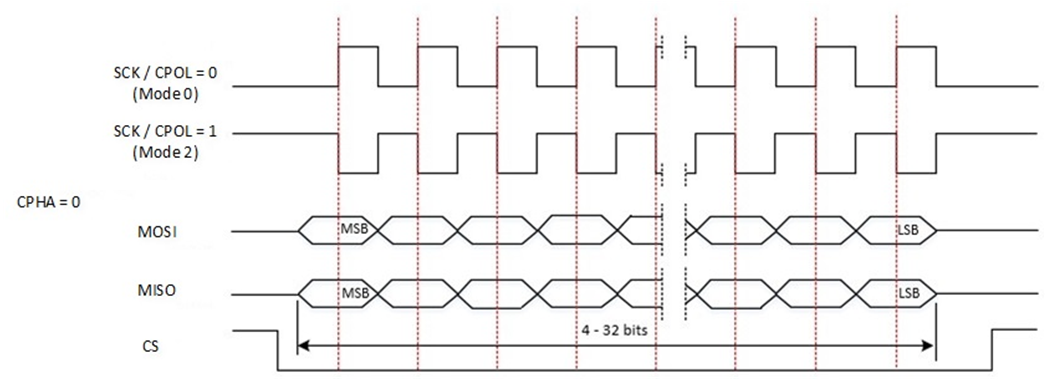
SPI Communication Sequence Diagram (SCPH is 0)
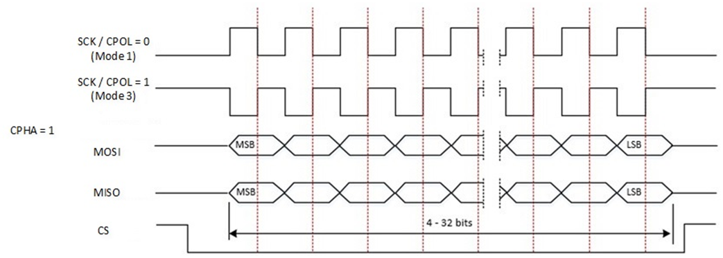
SPI Communication Sequence Diagram (SCPH is 1)
Program Examples
Initialization Flow
SPI initialization flow is shown in the following figure.
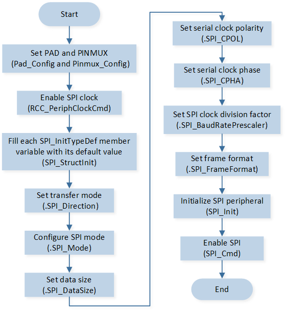
SPI Initialization Flow Chart
The codes below demonstrate the SPI initialization flow.
void driver_spi_init(void)
{
   /* turn on SPI clock */
   RCC_PeriphClockCmd(APBPeriph_SPI1, APBPeriph_SPI1_CLOCK, ENABLE);

   SPI_InitTypeDef  SPI_InitStructure;
   SPI_StructInit(&SPI_InitStructure);

   SPI_InitStructure.SPI_Direction   = SPI_Direction_FullDuplex;
   SPI_InitStructure.SPI_Mode        = SPI_Mode_Master;
   SPI_InitStructure.SPI_DataSize    = SPI_DataSize_8b;
   SPI_InitStructure.SPI_CPOL        = SPI_CPOL_High;
   SPI_InitStructure.SPI_CPHA        = SPI_CPHA_1Edge;
   SPI_InitStructure.SPI_BaudRatePrescaler  = 100;
   SPI_InitStructure.SPI_FrameFormat = SPI_Frame_Motorola;

   SPI_Init(SPI1, &SPI_InitStructure);
   SPI_Cmd(SPI1, ENABLE);
}
External Flash
This section introduces how to communicate with external flash by SPI. Please refer to SPI Demo Code 3 Description for demo code and refer to SPI Demo Code 3 Hardware Connection Diagram for hardware connection.
Hardware Connection
Users need to modify the pins related to external flash in the code according to the hardware design. The macro definition below shows the pins defined in the code.
#define FLASH_SCK                   P5_0
#define FLASH_MOSI                  P5_2
#define FLASH_MISO                  P5_3
#define FLASH_CS                    P5_1
#define FLASH_HOLD                  P5_5
Demo Code
Users can implement functions to communicate with external flash by referring to the demo code in SPI Demo Code 3 Description.
Commands for External Flash
Different flash models may have different commands, and users can modify the following definitions according to the flash specifications.
typedef enum
{
   EXT_FLASH_WRITE_STATUS_CMD      = 0x01,
   EXT_FLASH_PROGRAM_CMD           = 0x02,
   EXT_FLASH_READ_CMD              = 0x03,
   EXT_FLASH_WRITE_DISABLE_CMD     = 0x04,
   EXT_FLASH_READ_STATUS_CMD       = 0x05,
   EXT_FLASH_WRITE_ENABLE_CMD      = 0x06,
   EXT_FLASH_SECTOR_ERASE_CMD      = 0x20,
   EXT_FLASH_BLOCK_ERASE_32_CMD    = 0x52,
   EXT_FLASH_CHIP_ERASE_CMD        = 0x60,
   EXT_FLASH_BLOCK_ERASE_64_CMD    = 0xd8,
   EXT_FLASH_READ_ID_CMD           = 0x9F,
   EXT_FLASH_RELEASE_DEEP_SLEEP    = 0xAB,
   EXT_FLASH_DEEP_SLEEP            = 0xB9,
   EXT_FLASH_SOFTWARE_RESET_ENABLE = 0x66,
   EXT_FLASH_SOFTWARE_RESET        = 0x99,
} EXT_FLASH_OPERATION_CMD;
Initialization of External Flash
Users can refer to the following function to initialize external flash. In this function, it will initialize SPI and reset external flash.
void ext_flash_spi_init(void)
Erase External Flash
Users can refer to the following function to erase external flash. Sector, block, and chip are the three common erase commands used for flash.
EXT_FLASH_SPI_OPERATION_STATUS ext_flash_spi_erase(uint32_t address, EXT_FLASH_OPERATION_CMD mode)
Write External Flash
Users can refer to the following function to write external flash by polling mode.
EXT_FLASH_SPI_OPERATION_STATUS ext_flash_spi_page_program(uint32_t address, uint8_t *psendBuf, uint16_t len)
Users can refer to the following function to write external flash by interrupt mode.
Users can refer to the following function to write external flash by GDMA mode.
Read External Flash
Users can refer to the following function to read external flash by polling mode.
EXT_FLASH_SPI_OPERATION_STATUS ext_flash_spi_read(uint32_t address, uint8_t *pStoreBuf, uint16_t len)
Users can refer to the following function to read external flash by interrupt mode.
EXT_FLASH_SPI_OPERATION_STATUS ext_flash_spi_read_by_interrupt(uint32_t address, uint8_t *pStoreBuf, uint16_t len)
Users can refer to the following function to read external flash by GDMA mode.
EXT_FLASH_SPI_OPERATION_STATUS ext_flash_spi_read_by_dma(uint32_t address, uint8_t *pStoreBuf, uint16_t len)
Slave Note
The SPI slave does not support TX FIFO underflow conditions. The TX FIFO needs to be filled with data before the SPI master starts the transfer. There are two methods to avoid this condition:
Send data to the SPI slave TX FIFO before transmission, then toggle a GPIO to notify the SPI master to send data. For the specific implementation, please refer to the demo code in
src\sample\io_demo\spi\slave\spi_slave_gpio_demo.c.Use GDMA for the SPI slave to send data: Enable TX GDMA immediately after SPI slave init to ensure that there is always data in the SPI slave TX FIFO.
Note
If TX FIFO underflow occurs, users can reset SPI slave to recover.
For details, please refer to src\sample\io_demo\spi\slave\spi_slave_tx_dma_hs_demo.c.
GDMA Flow Based on GPIO Indication
This section introduces SPI slave transfers based on GPIO Indication when communicating with the SPI master in GDMA mode. The SPI slave must send data to the TX FIFO before the SPI master starts to communicate with the SPI slave; Otherwise, it will trigger TX FIFO underflow error interrupt for the SPI slave. Users can use GPIO to control the timing between the SPI master and the SPI slave. A GPIO pin needs to be toggled for the SPI slave to indicate that the TX data is ready, and the SPI master can transfer data afterward. For the detailed flow, please refer to SPI MISO Flow Chart.
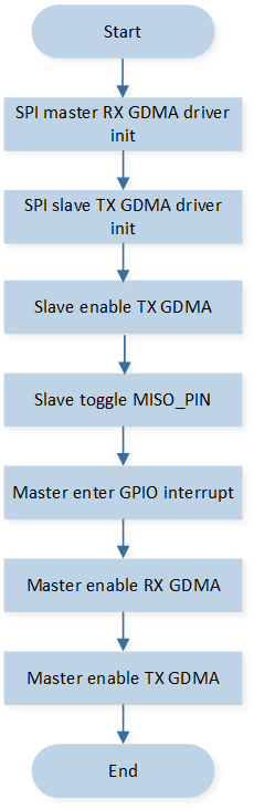
SPI MISO Flow Chart
GDMA Note
If SPI is operated in CPU mode with GDMA handshake enabled, it may cause GDMA to get the false signal. So if it’s needed for SPI to read or write by GDMA after CPU mode, the GDMA handshake must be reset before starting GDMA.
SPI_GDMACmd(FLASH_SPI, SPI_GDMAReq_Rx, DISABLE);
SPI_GDMACmd(FLASH_SPI, SPI_GDMAReq_Rx, ENABLE);
GDMA_Cmd(SPI_RX_DMA_CHANNEL_NUM, ENABLE);
Slave High Speed
The SPI slave needs to adjust the slow clock to support high speed, as shown in SPI Slow Clock Settings in RTL87x3E and SPI Slow Clock Settings in RTL87x3D.
For details, please refer to the demo code in src\sample\io_demo\spi\slave\spi_slave_tx_dma_hs_demo.c
and src\sample\io_demo\spi\slave\spi_slave_rx_dma_hs_demo.c.
SPI Clock Div |
SPI Clock |
Slave RX Slow Clock |
Slave TX Slow Clock |
|---|---|---|---|
16 |
2.5MHz |
/ |
1.25MHz |
10 |
4MHz |
/ |
1.25MHz |
8 |
5MHz |
/ |
2.5MHz |
4 |
10MHz |
2.5M |
4MHz |
SPI Clock Div |
SPI Clock |
Slave TX Slow Clock |
|---|---|---|
8 |
5MHz |
2.5MHz |
4 |
10MHz |
5MHz |