SDIO
SDIO Demo Code Support List
This chapter introduces the details of the SDIO demo code.
SDIO Demo for Read and Write
The description of SDIO demo code 1 is shown in the following table.
Demo 1 |
|
|---|---|
Sample Purpose |
|
Brief Introduction |
This sample code demonstrates SD card read and write function. Read the data at the specified address of the SD card, and write the specified data to the SD card. |
File Path |
|
Function Entry |
|
Supply Voltage |
3.3V, check MCU config of voltage setting. |
Group Pins |
The specific group pins are shown in SDIO Group Pins in RTL87x3D and SDIO Group Pins in RTL87x3E. |
Hardware Connection |
Take RTL87x3D group0 as an example, shown in SDIO Demo Code Hardware Connection Diagram. The 6 pins of the SD card are respectively connected with group0 on EVB, and the VDD and GND pins of the SD card are connected with the VCC and GND pins on EVB. |
Expected Result |
Press the Reset button on the EVB, the string sd_print_binary_data: buf will be printed in Debug Analyzer. The last printed data buf is 0~FF+0~FF (512 bytes). |
The hardware connection of SDIO demo code 1 is shown in the figure below.
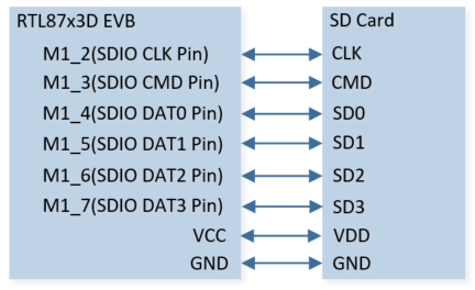
SDIO Demo Code Hardware Connection Diagram
The group pins of SDIO is shown in the tables below. RTL87x3EP is the same as RTL87x3E.
RTL87x3D |
CLK |
CMD |
DAT0 |
DAT1 |
DAT2 |
DAT3 |
|---|---|---|---|---|---|---|
Group0 Pins |
P1_2 |
P1_3 |
P1_4 |
P1_5 |
P1_6 |
P1_7 |
Group1 Pins |
P4_2 |
P4_3 |
P4_4 |
P4_5 |
P4_6 |
P4_7 |
RTL87x3E |
CLK |
CMD |
DAT0 |
DAT1 |
DAT2 |
DAT3 |
|---|---|---|---|---|---|---|
Group0 Pins |
P5_0 |
P5_1 |
P5_2 |
P5_3 |
P5_4 |
P5_5 |
Group1 Pins |
P6_0 |
P6_1 |
P6_2 |
P6_3 |
P6_4 |
P6_5 |
SDIO Demo for Filesystem
The description of SDIO demo code 2 is shown in the following table.
Demo 2 |
|
|---|---|
Sample Purpose |
Demonstrates how PC communicates with SD card by filesystem. |
Brief Introduction |
This sample code demonstrates SD card read and write function by filesystem.
|
File Path |
|
Function Entry |
|
Supply Voltage |
3.3V, check MCU config of voltage setting. |
Group Pins |
The specific group pins are shown in SDIO Group Pins in RTL87x3D and SDIO Group Pins in RTL87x3E. |
Hardware Connection |
Take RTL87x3D group0 as an example, shown in SDIO Demo Code Hardware Connection Diagram. The 6 pins of the SD card are respectively connected with group0 on EVB, and the VDD and GND pins of the SD card are connected with the VCC and GND pins on EVB. |
Expected Result |
|
SDIO Demo for SD Card Detection
The description of SDIO demo code 3 is shown in the following table.
Demo 3 |
|
|---|---|
Sample Purpose |
Demonstrates SD card detection by GPIO. |
Brief Introduction |
This sample code demonstrates the SD card detection function. Simulate SD card insertion and removal through GPIO. |
File Path |
|
Function Entry |
sdio_card_detect_demo() |
Supply Voltage |
3.3V, check MCU config of voltage setting. |
Selected Card Detect Pin |
|
Group Pins |
The specific group pins are shown in SDIO Group Pins in RTL87x3D and SDIO Group Pins in RTL87x3E. |
Hardware Connection |
Take RTL87x3D group0 as an example, shown in SDIO Demo Code Hardware Connection Diagram. The 6 pins of the SD card are respectively connected with group0 on EVB, and the VDD and GND pins of the SD card are connected with the VCC and GND pins on EVB. |
Expected Result |
Connect P0_3 with GND on EVB, the string gpio_isr_cb: card insert! will be printed in Debug Analyzer. Remove P0_3 from GND, the string gpio_isr_cb: card remove! will be printed in Debug Analyzer. |
Functional Overview
SDIO
Secure Digital Input and Output, defines a peripheral interface. SDIO card is an IO device that uses the SD bus and SD commands. The shape and interface of the SDIO card are compatible with the SD card, but it not only realizes the storage function, but also realizes other functions, such as Bluetooth, Wireless Fidelity, etc.
SDHC
SD host controller, the connection of SDHC and SD card is shown in SDHC and SD Card Connection Diagram. The host controls the internal operation of the SD card by reading/writing SDHC internal registers.
SDIO Transmission Mode
SPI mode, 1-bit mode (single-wire), 4-bit SD mode (four-wire). The pin definitions in different modes are shown in SDIO Pin Definitions in Different Modes.
SDIO Interface Definition (4-bit SD mode)
CLK
Host to card clock signal.
CMD
Bi-directional command/response signal.
DAT0-DAT3
4 Bi-directional data signals.
Note
Pins |
4-Bit Mode |
1-Bit Mode |
SPI Mode |
|---|---|---|---|
1 |
VCC |
VCC |
VCC |
2 |
VSS1 |
VSS1 |
VSS1 |
3 |
VSS2 |
VSS2 |
VSS2 |
4 |
CLK |
CLK |
CLK |
5 |
CMD |
CMD |
CS |
6 |
DAT0 |
DAT0 |
DAT0 |
7 |
DAT1 |
RSV |
DAT1 |
8 |
DAT2 |
RSV |
RSV |
9 |
DAT3/CD |
CD |
RSV |
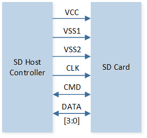
SDHC and SD Card Connection Diagram
Feature List
Support SD specifications V2.0.
Support only 2 group pins on EVB to communicate with SD card. For specific pins, please refer to SDIO Group Pins in RTL87x3D or SDIO Group Pins in RTL87x3E.
Support 1-bit and 4-bit SD bus width.
Support optional bus clock, 40MHz and 80MHz can only support in RTL87x3D.
Support multiple block and single block transfer, SDHC max block size is 512 Bytes.
High voltage SD card: operation voltage 3.3V.
Support GDMA transfer.
Support interrupt control.
SD Bus Protocol
The control on the SD bus is realized through CMD: The host initiates a request, and then the SD card responds to the request.
Data transfer format: Start bit 0, first MSB, then LSB, CRC check, end bit 1.
Data is transferred in the form of data blocks. SD Bus block read and write operation, as shown in SD BUS Multiple Block Read Operation and SD BUS Multiple Block Write Operation.
Take the SD Bus multi-block read operation as an example:
The host sends a multi-block read command.
The SD card sends a response.
The card starts sending data.
After each block is sent, return a CRC status.
The card transmits the next block data.
Until the host sends a stop command, the card responds.
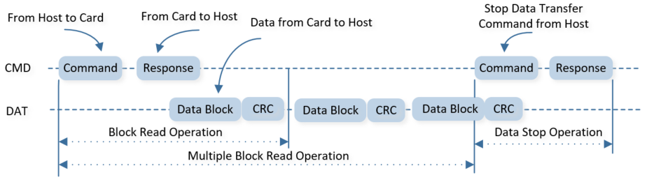
SD BUS Multiple Block Read Operation
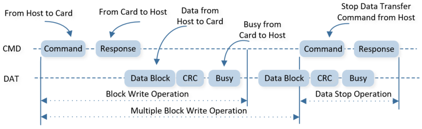
SD BUS Multiple Block Write Operation
Program Examples
Operation Flow
The codes below demonstrate the SD card initialization flow.
const T_SD_CONFIG    sd_card_cfg =
{
   .sd_if_type = SD_IF_SD_CARD,
   .sdh_group = GROUP_0,
   .sdh_bus_width = SD_BUS_WIDTH_4B,
   .sd_bus_clk_sel = SD_BUS_CLK_20M
};

/* SD config init */
sd_config_init((T_SD_CONFIG *)&sd_card_cfg);
/* Group pins PINMUX & PAD Config */
sd_board_init();
/* Initialize SD card peripheral */
sd_card_init();
The codes below demonstrate the SD card communication flow. For details, please refer to src\sample\io_demo\sdio\sdcard\sdio_demo.c.
static uint8_t *test_buf = NULL;
uint32_t sd_status = 0;

void sd_test(void)
{
   memset(test_buf, 0, sizeof(test_buf));
   /* Read the data at the specified address of the SD card */
   sd_status = sd_read(OPER_SD_CARD_ADDR, (uint32_t)test_buf, SINGLE_BLOCK_SIZE, BLOCK_NUM);

   if (sd_status != 0)
   {
      return ;
   }
   /*SD card print the binary data of test_buf */
   sd_print_binary_data(test_buf, SINGLE_BLOCK_SIZE * BLOCK_NUM);

   for (uint32_t i = 0; i < SINGLE_BLOCK_SIZE * BLOCK_NUM; i++)
   {
      test_buf[i] = i & 0xff;
   }
   sd_print_binary_data(test_buf, SINGLE_BLOCK_SIZE * BLOCK_NUM);
   /* Write the specified test_buf data to the SD card */
   sd_status = sd_write(OPER_SD_CARD_ADDR, (uint32_t)test_buf, SINGLE_BLOCK_SIZE, BLOCK_NUM);
}
The codes below demonstrate the SD card communication flow by filesystem.
For details, please refer to src\sample\io_demo\sdio\sdcard\demo\sdio_fs_demo.c.
void FatFS_Demo(void)
{
   uint32_t a = 1;
   uint32_t res = 0;
   const char driver_num = 0;

   /* Create workspace */
   res = f_mount(&fs, &driver_num, 1);

   /* Open file */
   res = f_open(&fdst, "Test.txt", FA_CREATE_ALWAYS | FA_WRITE);
   if (res != FR_OK)
   {
      //Open file failure, add error handle code here
      f_close(&fdst);
      return ;
   }

   res = f_open(&fsrc, "Data.txt", FA_OPEN_EXISTING | FA_READ);
   if (res != FR_OK)
   {
      //Open file failure, add error handle code here
      f_close(&fsrc);
      return ;
   }

   /* File operation */
   for (uint32_t i = 0; i < 1024; i++)
   {
      buffer[i] = i % 0x09 + 0x30;
   }
   buffer[1021] = 69;
   buffer[1022] = 69;
   buffer[1023] = 69;
   f_write(&fdst, buffer, 1024, &a);

   memset(buffer, 0, 1024);
   f_read(&fsrc, buffer, 1024, &a);

   /* Close file */
   f_close(&fsrc);
   f_close(&fdst);
}