I2S
Functional Overview
I2S interface can support audio protocols such as I2S, Left-Justified, PCM, and TDM. Through the I2S interface, RTL87x3E and RTL87x3D can bridge to an external DSP core (or audio codec/audio amplifier). I2S can be operated in GDMA mode or FIFO mode. Set the buffer size according to the amount of transferred data in GDMA mode, or access I2S FIFO directly to transmit and receive data in FIFO mode. It is recommended to transfer the audio data via GDMA automatically since it can reduce the number of interrupts and improve efficiency.
Feature List
Configurable BCLK and LRCK clock rate.
Support I2S, Left-Justified, PCM format.
Support 16/ 20/ 24/ 32 bits data resolution (data width).
Support 16/ 20/ 24/ 32 bits word length (channel width).
Support non-TDM (2-ch), TDM4 (4-ch), TDM6 (6-ch), and TDM8 (8-ch).
Support master and slave mode.
Support GDMA handshake operation.
Clock Divider
BCLK fractional divider according to the following equation:
BCLK = XTAL 40MHz * (I2S_BClockNi / I2S_BClockMi).Example: For XTAL 40MHz clock source to generate 12.288MHz BCLK case. It’s recommended to use the settings of
I2S_BClockNi = 192andI2S_BClockMi = 625.Note that because the clock source comes from XTAL 40MHz, BCLK would be a jittered clock composed of 10MHz and 13.33MHz in practice.
Set even-bit integer divider for LRCK according to the following equation:
LRCK = BCLK / (I2S_BClockDiv + 1).Where
I2S_BClockDivcould be calculated by:I2S_BClockDiv = (channel width * channel number) - 1.The channel number is determined by the TDM (Time Division Multiplexing) mode, 2-channels for without-TDM mode, 4-channels for TDM4 mode, and so on.
The recommended clock divider setting for 2-channels & 32-bit channel width is shown below.
BCLK Frequency |
Clock Source |
I2S_BClockNi |
I2S_BClockMi |
I2S_BClockDiv |
Sampling Rate |
0.512 MHz |
XTAL 40MHz |
8 |
625 |
63 |
8 KHz |
0.768 MHz |
XTAL 40MHz |
12 |
625 |
63 |
12 KHz |
1.024 MHz |
XTAL 40MHz |
16 |
625 |
63 |
16 KHz |
1.536 MHz |
XTAL 40MHz |
24 |
625 |
63 |
24 KHz |
2.048 MHz |
XTAL 40MHz |
32 |
625 |
63 |
32 KHz |
3.072 MHz |
XTAL 40MHz |
48 |
625 |
63 |
48 KHz |
6.144 MHz |
XTAL 40MHz |
96 |
625 |
63 |
96 KHz |
12.288 MHz |
XTAL 40MHz |
192 |
625 |
63 |
192 KHz |
2.8224 MHz |
XTAL 40MHz |
441 |
6250 |
63 |
44.1 KHz |
5.6448 MHz |
XTAL 40MHz |
441 |
3125 |
63 |
88.2 KHz |
0.7056 MHz |
XTAL 40MHz |
441 |
25000 |
63 |
11.025 KHz |
1.4112 MHz |
XTAL 40MHz |
441 |
12500 |
63 |
22.05 KHz |
As mentioned above, I2S BCLK is a jittered clock composed of two frequencies that are generated from XTAL 40MHz. The clock jitter percentage generated from XTAL 40MHz is shown in below.
BCLK (MHz) |
Clock Jitter Percentage (%) |
|
Sampling Rate 48KHz Group |
1.024 |
1.132 |
2.048 |
1.032 |
|
3.072 |
1.772 |
|
6.144 |
1.297 |
|
12.288 |
1.627 |
|
Sampling Rate 44.1KHz Group |
2.8224 |
1.241 |
5.6448 |
1.261 |
|
11.2896 |
1.24 |
LRCK (KHz) |
Clock Jitter Percentage (%) |
16 |
0 |
48 |
0.08 |
96 |
0.179 |
44.1 |
0.107 |
88.2 |
0.114 |
192 |
0.168 |
Program Examples
Initialization Flow
I2S function initialization flow is shown in the following figure.
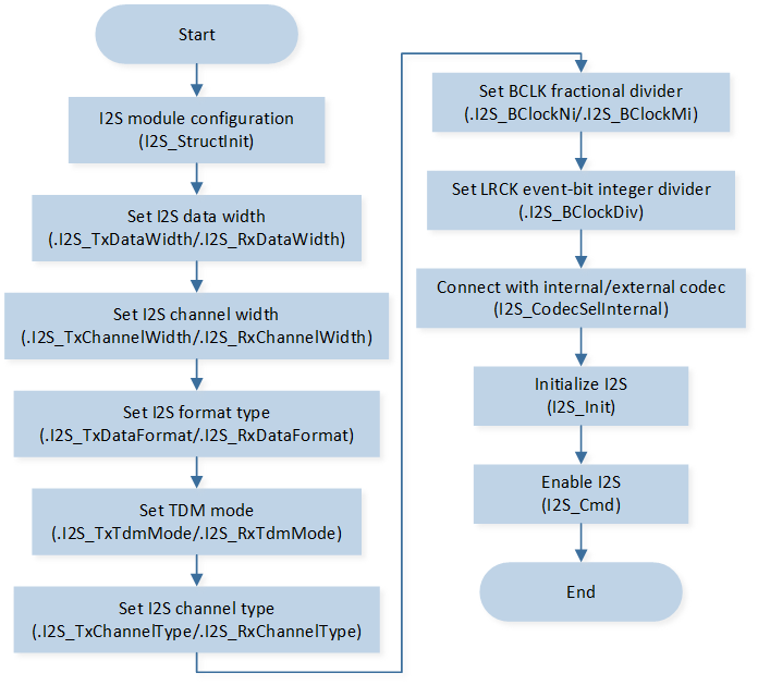
I2S Init Flow
The codes below demonstrate the I2S function initialization flow.
Note
As mentioned in PINMUX and PAD function descriptions, I2S PAD should be configured as software mode and pulled down when I2S is disabled to prevent PAD from floating during low power mode.
void board_i2s_init(void)
{
   /* set PAD_SW_MODE & PAD_PULL_DOWN when I2S is disabled to prevent PAD floating in low power mode */
   Pad_Config(I2S_BCLK_PIN, PAD_PINMUX_MODE, PAD_IS_PWRON, PAD_PULL_NONE, PAD_OUT_ENABLE, PAD_OUT_LOW);
   Pad_Config(I2S_LRCK_PIN, PAD_PINMUX_MODE, PAD_IS_PWRON, PAD_PULL_NONE, PAD_OUT_ENABLE, PAD_OUT_LOW);
   Pad_Config(I2S_SDO_PIN, PAD_PINMUX_MODE, PAD_IS_PWRON, PAD_PULL_NONE, PAD_OUT_ENABLE, PAD_OUT_LOW);
   Pad_Config(I2S_SDI_PIN, PAD_PINMUX_MODE, PAD_IS_PWRON, PAD_PULL_NONE, PAD_OUT_ENABLE, PAD_OUT_LOW);

   Pinmux_Config(I2S_BCLK_PIN, I2S_BCLK_PINMUX);
   Pinmux_Config(I2S_LRCK_PIN, I2S_LRCK_PINMUX);
   Pinmux_Config(I2S_SDO_PIN, I2S_SDO_PINMUX);
   Pinmux_Config(I2S_SDI_PIN, I2S_SDI_PINMUX);
}

void driver_i2s_init(void)
{
   I2S_InitTypeDef I2S_InitStruct;

   I2S_StructInit(&I2S_InitStruct);
   I2S_InitStruct.I2S_ClockSource      = I2S_CLK_XTAL;
   /* BCLK = 40MHz * (I2S_BClockNi / I2S_BClockMi), LRCK = BCLK / (I2S_BClockDiv + 1) */
   I2S_InitStruct.I2S_BClockMi         = 0x271;    /* LRCK = 48KHz */
   I2S_InitStruct.I2S_BClockNi         = 0x30;     /* BCLK = 3.072MHz */
   I2S_InitStruct.I2S_BClockDiv        = 0x3F;
   I2S_InitStruct.I2S_DeviceMode       = I2S_DeviceMode_Master;
   I2S_InitStruct.I2S_TxChannelType    = I2S_Channel_Stereo;
   I2S_InitStruct.I2S_TxDataWidth      = I2S_Width_24Bits;
   I2S_InitStruct.I2S_RxDataWidth      = I2S_Width_24Bits;
   I2S_InitStruct.I2S_TxChannelWidth   = I2S_Width_32Bits;
   I2S_InitStruct.I2S_RxChannelWidth   = I2S_Width_32Bits;
   I2S_InitStruct.I2S_TxDataFormat     = I2S_Mode;
   I2S_InitStruct.I2S_RxDataFormat     = I2S_Mode;
   I2S_InitStruct.I2S_DMACmd           = I2S_DMA_DISABLE;
   I2S_Init(I2S_NUM, &I2S_InitStruct);

   I2S_Cmd(I2S_NUM, I2S_MODE_TRX, ENABLE);
}
Operation Flow
TX GDMA Handshake Operation
Turn on the peripheral clock source of the GDMA.
I2S TX and GDMA initialization: Set GDMA handshake with I2S TX.
Enable the
GDMA_INT_Transferinterrupt and enable GDMA.Invoke
I2S_Cmdto generate LRCK and start retrieving data from TX FIFO.Initiate GDMA request if TX FIFO water level is lower than TX GDMA burst size.
Trigger GDMA transfer interrupt and wait for GDMA transfer to complete.
Clear
GDMA_INT_Transferinterrupt.
The flow chart of I2S TX GDMA handshake operation is shown in the following figure.
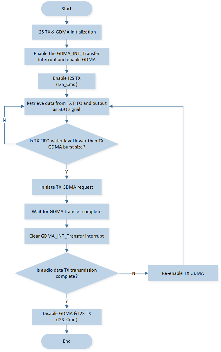
I2S TX GDMA Flow
RX GDMA Handshake Operation
Turn on the peripheral clock source of the GDMA.
I2S RX and GDMA initialization: Set GDMA handshake with I2S RX.
Enable the
GDMA_INT_Transferinterrupt and enable GDMA.Invoke
I2S_Cmdto generate LRCK and start sending data to RX FIFO.Wait for RX FIFO data to exceed RX GDMA burst size and initiate GDMA request.
Trigger GDMA transfer interrupt and wait for GDMA transfer to complete.
Clear
GDMA_INT_Transferinterrupt.
The flow chart of I2S RX GDMA handshake operation is shown in the following figure.
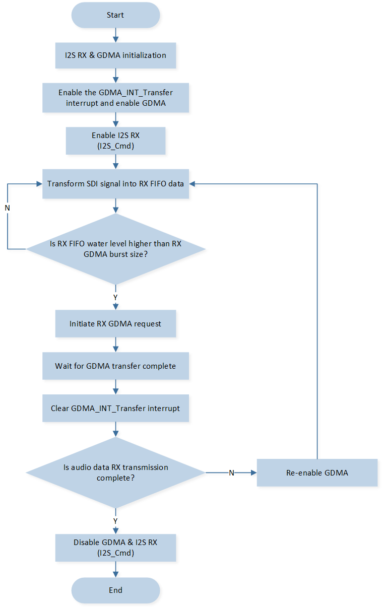
I2S RX GDMA Flow
The codes below demonstrate the I2S GDMA handshake initialization flow.
void driver_gdma_init(T_I2S_CONFIG_DIR dir)
{
   GDMA_InitTypeDef gdma_init;
   NVIC_InitTypeDef nvic_init;

   RCC_PeriphClockCmd(APBPeriph_GDMA, APBPeriph_GDMA_CLOCK, ENABLE);

   GDMA_StructInit(&gdma_init);
   gdma_init.GDMA_BufferSize           = I2S_DMA_BUF_LEN;
   gdma_init.GDMA_SourceDataSize       = GDMA_DataSize_Word;
   gdma_init.GDMA_DestinationDataSize  = GDMA_DataSize_Word;
   gdma_init.GDMA_SourceMsize          = GDMA_Msize_4;
   gdma_init.GDMA_DestinationMsize     = GDMA_Msize_4;

   if (dir == I2S_CONFIG_TX)
   {
      gdma_init.GDMA_ChannelNum           = I2S_TX_DMA_CHANNEL_NUM;
      gdma_init.GDMA_DIR                  = GDMA_DIR_MemoryToPeripheral;
      gdma_init.GDMA_SourceAddr           = (uint32_t)(i2s_send_buff);
      gdma_init.GDMA_DestinationAddr      = (uint32_t)I2S_TX_ADDR;
      gdma_init.GDMA_SourceInc            = DMA_SourceInc_Inc;
      gdma_init.GDMA_DestinationInc       = DMA_DestinationInc_Fix;
      gdma_init.GDMA_DestHandshake        = I2S_TX_DMA_HANDSHAKE;
      GDMA_Init(I2S_TX_DMA_CHANNEL, &gdma_init);

      RamVectorTableUpdate(I2S_TX_DMA_VECTOR, i2s_tx_dma_handler);

      nvic_init.NVIC_IRQChannel           = I2S_TX_DMA_IRQ;
   }
   else if (dir == I2S_CONFIG_RX)
   {
      gdma_init.GDMA_ChannelNum           = I2S_RX_DMA_CHANNEL_NUM;
      gdma_init.GDMA_DIR                  = GDMA_DIR_PeripheralToMemory;
      gdma_init.GDMA_SourceAddr           = (uint32_t)I2S_RX_ADDR;
      gdma_init.GDMA_DestinationAddr      = (uint32_t)(i2s_recv_buff);
      gdma_init.GDMA_SourceInc            = DMA_SourceInc_Fix;
      gdma_init.GDMA_DestinationInc       = DMA_DestinationInc_Inc;
      gdma_init.GDMA_SourceHandshake      = I2S_RX_DMA_HANDSHAKE;
      GDMA_Init(I2S_RX_DMA_CHANNEL, &gdma_init);

      RamVectorTableUpdate(I2S_RX_DMA_VECTOR, i2s_rx_dma_handler);

      nvic_init.NVIC_IRQChannel           = I2S_RX_DMA_IRQ;
   }

   nvic_init.NVIC_IRQChannelCmd        = (FunctionalState)ENABLE;
   nvic_init.NVIC_IRQChannelPriority   = 3;
   NVIC_Init(&nvic_init);
}